PNX1311EH/G,557 NXP Semiconductors, PNX1311EH/G,557 Datasheet
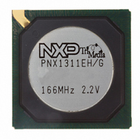
PNX1311EH/G,557
Specifications of PNX1311EH/G,557
935277721557
PNX1311EH/G


Related parts for PNX1311EH/G,557


PNX1311EH/G,557 Summary of contents
Page 1
PNX1300 Series Media Processors Preliminary Specification Supersedes PNX1300 data of 2001 Oct 12 File under INTEGRATED CIRCUITS, TR1 INTEGRATED CIRCUITS 2002 Feb 15 ...
Page 2
Philips Semiconductors Media Processors 2002 Feb 15 Preliminary Specification PNX1300 Series ...
Page 3
PNX1300 Series Data Book Foreword Table of Contents 1 Pin List 2 Overview 3 DSPCPU Architecture 4 Custom Operations for Multimedia 5 Cache Architecture 6 Video In 7 Enhanced Video Out 8 Audio In 9 Audio Out 10 SPDIF Out ...
Page 4
Terms and Conditions TERMS AND CONDITIONS Philips Semiconductors and Philips Electronics North America Corporation reserve the right to make changes, without notice, in the products, including circuits, standard cells, and/or software, described or contained herein in order to improve design ...
Page 5
Foreword The TriMedia PNX1300 Series is an enhanced version of the TM-1300 family of media processor. The PNX1300 Series contains an ultra-high performance Very Long Instruction Word processor, as well as a com- plete intelligent video and audio input/output subsystem. ...
Page 6
PNX1300/01/02/11 Data Book 2 PRELIMINARY INFORMATION Philips Semiconductors ...
Page 7
Table of Contents Foreword 1 Pin List 1.1 PNX1300 Series versus TM-1300 . . . . . . . . . . . . . . . . . . . . . . . . . . . . ...
Page 8
PNX1300/01/02/11 Data Book 2 Overview 2.1 Introduction . . . . . . . . . . . . . . . . . . . . . . . . . . . . . . . . . ...
Page 9
Philips Semiconductors 3.3 PNX1300 Instruction Issue Rules . . . . . . . . . . . . . . . . . . . . . . . . . . . . . . . . . ...
Page 10
PNX1300/01/02/11 Data Book 5.3.3 Miss Processing Order . . . . . . . . . . . . . . . . . . . . . . . . . . . . . . . . . ...
Page 11
Philips Semiconductors 5.7 Performance Evaluation Support . . . . . . . . . . . . . . . . . . . . . . . . . . . . . . . . . . ...
Page 12
PNX1300/01/02/11 Data Book 7.12.1 Video Image Formats . . . . . . . . . . . . . . . . . . . . . . . . . . . . . . . . . ...
Page 13
Philips Semiconductors 8.10 Error Behavior . . . . . . . . . . . . . . . . . . . . . . . . . . . . . . . . . . . ...
Page 14
PNX1300/01/02/11 Data Book 10.16 Power Down and Sleepless . . . . . . . . . . . . . . . . . . . . . . . . . . . . . . . . ...
Page 15
Philips Semiconductors 11.6.11 IO_ADR Register . . . . . . . . . . . . . . . . . . . . . . . . . . . . . . . . . . . ...
Page 16
PNX1300/01/02/11 Data Book 12.15.3 Termination . . . . . . . . . . . . . . . . . . . . . . . . . . . . . . . . . . . ...
Page 17
Philips Semiconductors 14.5.2 Filtering . . . . . . . . . . . . . . . . . . . . . . . . . . . . . . . . . . . . ...
Page 18
PNX1300/01/02/11 Data Book 15.4 VLD Input . . . . . . . . . . . . . . . . . . . . . . . . . . . . . . . . . . ...
Page 19
Philips Semiconductors 17.2 Interface . . . . . . . . . . . . . . . . . . . . . . . . . . . . . . . . . . . . ...
Page 20
PNX1300/01/02/11 Data Book 19.2 SEM Device Specification . . . . . . . . . . . . . . . . . . . . . . . . . . . . . . . . . ...
Page 21
Philips Semiconductors 22.5.1 PCI_CLK Bus Clock Frequency . . . . . . . . . . . . . . . . . . . . . . . . . . . . . . . . . ...
Page 22
PNX1300/01/02/11 Data Book dualiclipi . . . . . . . . . . . . . . . . . . . . . . . . . . . . . . . . . . . . ...
Page 23
Philips Semiconductors iaddi . . . . . . . . . . . . . . . . . . . . . . . . . . . . . . . . . . . . . ...
Page 24
PNX1300/01/02/11 Data Book imin . . . . . . . . . . . . . . . . . . . . . . . . . . . . . . . . . . . . ...
Page 25
Philips Semiconductors readpcsw . . . . . . . . . . . . . . . . . . . . . . . . . . . . . . . . . . . . . ...
Page 26
PNX1300/01/02/11 Data Book uleqi . . . . . . . . . . . . . . . . . . . . . . . . . . . . . . . . . . . . ...
Page 27
Pin List 1.1 PNX1300 SERIES VERSUS TM-1300 The following summarizes differences between TM-1300 and PNX1300/01/02/11: • Lower core voltage for PNX1311 (2.2V core voltage) and therefore lower power consumption. • DSPCPU speed 200 MHz. • SDRAM speed ...
Page 28
PNX1300/01/02/11 Data Book 1.4 SIGNAL PIN LIST In the table below, a pin name ending in a ‘#’ designates an active-low signal (the active state of the signal is a low voltage level). All other signals have active-high polarity. BGA ...
Page 29
Philips Semiconductors BGA Pad Pin Name Mode Ball Type MM_CLK0 Y10 STRG3 MM_CLK1 W10 MM_A00 W12 NORM3 MM_A01 Y12 MM_A02 W11 MM_A03 Y11 MM_A04 Y9 MM_A05 W9 MM_A06 V9 MM_A07 Y8 MM_A08 W8 MM_A09 Y7 MM_A10 V12 MM_A11 Y13 MM_A12 ...
Page 30
PNX1300/01/02/11 Data Book BGA Pad Pin Name Mode Ball Type MM_DQM0 T19 NORM3 MM_DQM1 R18 MM_DQM2 V1 MM_DQM3 V4 PCI Interface (Note: current buffer design allows drive/receive from either 3 PCI bus) PCI_CLK T2 PCI PCI_AD00 T1 PCI ...
Page 31
Philips Semiconductors BGA Pad Pin Name Mode Ball Type PCI_INTA# C9 PCIOD PCI_INTB# A8 PCI I/O/OD PCI_INTC# B8 PCIOD PCI_INTD# A7 PCIOD JTAG Interface (debug access port and 1149.1 boundary scan port) JTAG_TDI F20 WEAK5 JTAG_TDO F18 WEAK5 JTAG_TCK F19 ...
Page 32
PNX1300/01/02/11 Data Book BGA Pad Pin Name Mode Ball Type VO_IO1 J18 WEAK5 VO_IO2 H20 WEAK5 VO_CLK J19 STRG5 Audio In (always acts as receiver, but can be master or slave for A/D timing) AI_OSCLK B15 STRG3 AI_SCK A16 STRG5 ...
Page 33
Philips Semiconductors BGA Pad Pin Name Mode Ball Type Audio Out (always acts as sender, but can be master or slave for D/A timing) AO_OSCLK B14 STRG3 AO_SCK A14 STRG5 AO_SD1 B13 WEAK5 AO_SD2 A13 WEAK5 OUT AO_SD3 C12 WEAK5 ...
Page 34
PNX1300/01/02/11 Data Book 1.5 POWER PIN LIST VSS (ground C16 H9 L10 D4 H10 L11 D5 H11 L12 D16 H12 L13 D17 H13 M10 E17 J10 M11 E18 J11 M12 T3 ...
Page 35
Philips Semiconductors 1.6 PIN REFERENCE VOLTAGE With the exception of Open Drain mode outputs, outputs always drive to a level determined by the 3.3-V I/O voltage. VREF_PERIPH and VREF_PCI purely determine input voltage clamping, not input signal thresholds or output ...
Page 36
PNX1300/01/02/11 Data Book 1.7 PACKAGE HBGA292: plastic, heatsink ball grid array package; 292 balls; body 1.75 mm ball A1 index area ...
Page 37
Philips Semiconductors 1.9 PARAMETRIC CHARACTERISTICS 1.9.1 PNX1300/01/02/11 Absolute Maximum Ratings Permanent damage may occur if these conditions are exceeded Symbol V 2.5-V core supply voltage (PNX1300/01/02/11) DDMAX V 3.3-V I/O supply voltage CCMAX V DC input voltage on all 5-V ...
Page 38
PNX1300/01/02/11 Data Book 1.9.5 PNX1300/01/02 DC/AC Characteristics Symbol Parameter V Core supply voltage DD V I/O supply voltage CC I Core supply current DD-typ I I/O supply current CC-typ I Core supply current DD-pdn I I/O supply current CC-pdn V ...
Page 39
Philips Semiconductors 1.9.7 PNX1300 Series Power Consumption The power consumption of PNX1300 Series is depen- dent on the activity of the DSPCPU, the amount of pe- ripherals being used, the frequency at which the system is running as well as ...
Page 40
PNX1300/01/02/11 Data Book 1.9.7.2 PNX1300/01/02 DSPCPU Core Current and Power Consumption Symbol Current/Notes PNX130x I DD (note Total Power Dissipation I , DSPCPU Only DSPCPU Only CC Power DSPCPU Only PNX130x I , Standby ...
Page 41
Philips Semiconductors 1.9.7.4 PNX1300/01/02 Current Consumption For On-Chip Peripherals Symbol Current/Notes Pwd running raw mode DD 27 MHz I , running raw mode running raw mode DD 81 MHz I , running raw ...
Page 42
PNX1300/01/02/11 Data Book 1.9.7.5 PNX1311 Current Consumption For On-Chip Peripherals PNX1311-100:100 Symbol Current/Notes Pwd running raw mode DDL 27 MHz I , running raw mode running raw mode DDL 81 MHz I , ...
Page 43
Philips Semiconductors 1.9.7.6 STRG3, STRG5 type I/O circuit Symbol Parameter V Output HIGH voltage I OH OUT V Output LOW voltage I OL OUT Z Output AC impedance HIGH level output state OH Z Output AC impedance LOW level output ...
Page 44
PNX1300/01/02/11 Data Book 1.9.7.10 SDRAM interface timing for PNX1300/01/02/11 speed grades. Symbol Parameter f MM_CLK frequency SDRAM T Skew between MM_CLK0, CLK1 CS T Propagation delay of data, address, control PD T Output hold time of data, address and control ...
Page 45
Philips Semiconductors 1.9.7.12 JTAG I/O timing Symbol f JTAG clock frequency JTAG-CLK T JTAG_TCK to JTAG_TDO valid delay clk-TDO T Input setup time to JTAG_TCK su-TCK T Input hold time from JTAG_TCK h-TCK Notes: 1. See the timing measurement conditions ...
Page 46
PNX1300/01/02/11 Data Book 1.9.7.16 AudioIn I/O timing Symbol f Audio In AI_SCK clock frequency AI-SCK T Input setup time to AI_SCK su-SCK T Input hold time from AI_SCK h-SCK T AI_SCK to AI_WS SCK-WS Notes: 1. See the timing measurement ...
Page 47
Philips Semiconductors PNX1300 pin 2” true length 30-ohm Output 50-ohm Buffer Figure 1-1. STRG3, STRG5 test load circuit PNX1300 pin 2” true length Output 50-ohm Buffer Figure 1-2. NORM3 test load circuit PNX1300 pin 2” true length Output 50-ohm Buffer ...
Page 48
PNX1300/01/02/11 Data Book TCK T clk_TDO valid TDO Figure 1-10. JTAG Output Timing T T HIGH LOW SCL Figure 1-11 I/O Timing SCL T TBUF SDA 2 Figure 1-12 I/O Timing SCL T ...
Page 49
Philips Semiconductors AI_SCK AI_WS Figure 1-20. Audio In I/O Timing AO_SCK AO_SDx Figure 1-21. Audio Out I/O Timing AO_SCK AO_WS Figure 1-22. Audio Out I/O Timing AO_SCK T SCK_WS valid AO_WS Figure 1-23. Audio Out I/O Timing SSI_CLK T SCK_DV ...
Page 50
PNX1300/01/02/11 Data Book 1-24 PRELIMINARY SPECIFICATION Philips Semiconductors ...
Page 51
Overview 2.1 INTRODUCTION In this document, the generic PNX1300 name refers to the PNX1300 Series, or the PNX1300/01/02/11 products. PNX1300 is a successor to the TM-1300, TM-1100 and TM-1000 media processors. For those familiar with the TM-1300, the new features ...
Page 52
PNX1300/01/02/11 Data Book • A high-performance bus and memory system that provide communication between PNX1300’s pro- cessing units. • A flexible external bus interface. Figure 2-1 shows a PNX1300 block diagram. The bulk of a PNX1300 system consists of the ...
Page 53
Philips Semiconductors Finally, the Synchronous Serial Interface (SSI) requires only an external ISDN or analog modem front-end chip and phone line interface to provide remote communica- tion support. It can be used to connect PNX1300-based systems for video phone or ...
Page 54
PNX1300/01/02/11 Data Book 2.5.2 VLIW Processor Core The heart of PNX1300 is a powerful 32-bit DSPCPU core. The DSPCPU implements a 32-bit linear address space and 128, fully general-purpose 32-bit registers. The registers are not separated into banks; any opera- ...
Page 55
Philips Semiconductors PC Screen FrameMaker 5 File Edit Format View IMAGE 1 Calendar File Edit Image 2 Image 1 Figure 2-3. ICP - Windows on the PC screen and data structures in SDRAM for two live video windows. window on ...
Page 56
PNX1300/01/02/11 Data Book 2.5.7 Audio In and Audio Out Units The Audio In (AI) and Audio Out (AO) units are similar to the video units. They connect to most serial ADC and DAC chips, and are programmable enough to handle ...
Page 57
DSPCPU Architecture 3.1 BASIC ARCHITECTURE CONCEPTS In the document the generic PNX1300 product name refers to PNX1300 Series, or the PNX1300/01/02/11 products. This section documents the system programmer or ‘bare-machine’ view of the PNX1300 CPU (or DSPCPU). 3.1.1 Register Model ...
Page 58
PNX1300/01/02/11 Data Book 3.1.2 Basic DSPCPU Execution Model The DSPCPU issues one ‘long instruction’ every clock cycle. Each instruction consists of several operations (five operations for the PNX1300 microprocessor). Each operation is comparable to a RISC machine instruction, except that ...
Page 59
Philips Semiconductors Table 3-2. PCSW FP exception flag definitions Flag Function INV Standard IEEE invalid flag OVF Standard IEEE overflow flag UNF Standard IEEE underflow flag INX Standard IEEE inexact flag DBZ Standard IEEE divide-by-zero flag OFZ ‘Output flushed to ...
Page 60
PNX1300/01/02/11 Data Book 3.1.7 Integer Representation The architecture supports the notion of 'unsigned inte- gers' and 'signed integers.' Signed integers use the stan- dard two’s-complement representation. Arithmetic on integers does not generate traps result is not representable, the ...
Page 61
Philips Semiconductors 3.2 INSTRUCTION SET OVERVIEW 3.2.1 Guarding (Conditional Execution) In the PNX1300 architecture, all operations can be op- tionally 'guarded'. A guarded operation executes condi- tionally, depending on the value in the ‘guard' register. For example, a guarded add ...
Page 62
PNX1300/01/02/11 Data Book 3.2.3 Compute Operations Compute operations are register-to-register operations. The specified operation is performed on one or two source registers and the result is written to the destina- tion register. Immediate Operations. Immediate operations load an immediate constant ...
Page 63
Philips Semiconductors • functional units should be ‘recovered’ from any prior operation issues Writeback constraint: • No more than 5 results should be simultaneously written to the register file at any point in time (write- back occurs ‘latency’ cycles after ...
Page 64
PNX1300/01/02/11 Data Book for PC-hosted PNX1300 boards; its final location is de- termined by the boot EEPROM for standalone systems. See Chapter 13, “System Boot” for more information. Figure 3-5 gives a detailed overview of the MMIO mem- ory map ...
Page 65
Philips Semiconductors The instruction scheduler uses interruptible jumps exclu- sively for inter-decision tree jumps. Hence, within a deci- sion tree, no special-event processing can be initiated tree-to-tree jump is taken, special-event processing is allowed. Since the only registers ...
Page 66
PNX1300/01/02/11 Data Book Programmer’s note: See the Philips TriMedia Cookbook (Book 2 of TriMedia SDE documentation) for information on writing interrupt handlers. 3.5.3.2 Interrupt modes DSPCPU interrupt sources can be programmed to oper- ate in either level-sensitive or edge-triggered mode. ...
Page 67
Philips Semiconductors device events lead to the request of an interrupt. In addi- tion, the PCSW.IEN flag determines whether the DSPCPU is willing to handle regular interrupts. Non maskable interrupts ignore the state of this flag. All three mechanisms are ...
Page 68
PNX1300/01/02/11 Data Book MMIO_BASE offset: 0x10 3038 INT_CTL (r/w) Figure 3-9. Host interrupt control register Table 3-10. Interrupt source assignments SOURCE SRC MODE SOURCE DESCRIPTION NAME NUM PCI INTA 0 level PCI_INTA# pin signal PCI INTB 1 level PCI_INTB# pin ...
Page 69
Philips Semiconductors Timer base offset: 0 TMODULUS (r/w) 4 TVALUE (r/w) 8 TCTL (r/w) Figure 3-10. Timer register definitions. Table 3-11. Timer base MMIO address TIMER1 MMIO_BASE+0x10,0C00 TIMER2 MMIO_BASE+0x10,0C20 TIMER3 MMIO_BASE+0x10,0C40 SYSTIMER MMIO_BASE+0x10,0C60 Table 3-12. Timer source selections Source Source ...
Page 70
PNX1300/01/02/11 Data Book MMIO_BASE offset: 0x10 1000 BICTL (r/w) Figure 3-11. Instruction-breakpoint control register. MMIO_BASE offset: 0x10 1004 BINSTLOW (r/w) 0x10 1008 BINSTHIGH (r/w) Figure 3-12. Instruction-breakpoint address-range registers. MMIO_BASE offset: 0x10 1030 BDATAALOW (r/w) 0x10 1034 BDATAAHIGH (r/w) 0x10 ...
Page 71
Philips Semiconductors Note that this comparison works for all addresses re- gardless of the aperture to which they belong. When the value of the DC bits is ‘2’ or ‘3’, any data value from load operations (if the BL bit ...
Page 72
PNX1300/01/02/11 Data Book 3-16 PRELIMINARY SPECIFICATION Philips Semiconductors ...
Page 73
Custom Operations for Multimedia 4.1 CUSTOM OPERATIONS OVERVIEW In this document, the generic PNX1300 name refers to the PNX1300 Series, or the PNX1300/01/02/11 products. Custom operations in the PNX1300 DSPCPU architec- ture are specialized, high-function operations designed to dramatically improve ...
Page 74
PNX1300/01/02/11 Data Book Table 4-1. Key Multimedia Custom Operations Listed by Function Type Function Custom Op DSP dspiabs Clipped signed 32-bit absolute absolute value value dspidualabs Dual clipped absolute values of signed 16-bit halfwords Shift dualasr dual-16 arithmetic shift right ...
Page 75
Philips Semiconductors Table 4-2. Key Multimedia Custom Operations Listed by Operand Size Op. Size Custom Op 8-bit quadumax Unsigned bytewise quad max quadumin Unsigned bytewise quad min dspuquadaddui Quad clipped add of unsigned/ signed bytes ifir8ii Signed sum of products ...
Page 76
PNX1300/01/02/11 Data Book ld32d(0) r100 r10 ld32d(4) r100 r11 ld32d(8) r100 r12 ld32d(12) r100 r13 mergemsb r10 r11 mergemsb r12 r13 mergelsb r10 r11 mergelsb r12 r13 pack16msb r14 r15 pack16lsb r14 r15 pack16msb r16 r17 pack16lsb r16 r17 st32d(0) ...
Page 77
Philips Semiconductors void reconstruct (unsigned char *back, { int i, temp; for ( < 64 Figure 4-4. Straightforward code for MPEG frame reconstruction. A straightforward coding of the reconstruction algorithm might ...
Page 78
PNX1300/01/02/11 Data Book void reconstruct (unsigned char *back, { int i, temp; for ( < 64 temp = ((back[i+0] + forward[i+ >> idct[i+0]; if (temp > 255) temp = ...
Page 79
Philips Semiconductors void reconstruct (unsigned char *back, { int i, temp0, temp1, temp2, temp3; for ( < 64 temp0 = ((back[i+0] + forward[i+ >> 1); temp1 = ((back[i+1] + forward[i+1] + ...
Page 80
PNX1300/01/02/11 Data Book void reconstruct (unsigned char *back, unsigned char *forward, unsigned char *destination) { int i; int *i_back = (int *) back; int *i_forward = (int *) forward; int *i_idct = (int *) idct; int *i_dest = (int *) ...
Page 81
Philips Semiconductors unsigned char A[16][16]; unsigned char B[16][16 for (row = 0; row < 16; row += 1) { for (col = 0; col < 16; col += 4) { cost0 = abs(A[row][col+0] – B[row][col+0]); cost1 = ...
Page 82
PNX1300/01/02/11 Data Book unsigned int *IA = (unsigned int *) A; unsigned int *IB = (unsigned int *) B; for (row = 0; row < 16; row += 1) { int rowoffset = row * 4; for (col4 = 0; ...
Page 83
Cache Architecture 5.1 MEMORY SYSTEM OVERVIEW In this document, the generic PNX1300 name refers to the PNX1300 Series, or the PNX1300/01/02/11 products. The high-performance video and audio throughput of PNX1300 is implemented by its DSPCPU and autono- mous I/O and ...
Page 84
PNX1300/01/02/11 Data Book the majority of instructions and data to the DSPCPU. The wide paths to the caches are matched to the bandwidth requirements of the DSPCPU. Table 5-2. Summary of memory system characteristics Unit Description Branch units Branch units ...
Page 85
Philips Semiconductors 5.3 DATA CACHE The data cache serves only the DSPCPU and is con- trolled by two memory units that execute the load and store operations issued by the DSPCPU. The following sections describe the data cache and its ...
Page 86
PNX1300/01/02/11 Data Book 5.3.3 Miss Processing Order When a miss occurs, the data cache fills the block con- taining the requested word from the critical word first. The CPU is stalled until the first word is transferred. The block is ...
Page 87
Philips Semiconductors MMIO_BASE offset: 0x10 0010 DC_LOCK_CTL (r/w) 0x10 0014 DC_LOCK_ADDR (r/w) 0x10 0018 DC_LOCK_SIZE (r/w) Figure 5-5. Formats of the registers in charge of data-cache locking. ‘1’. Setting DC_LOCK_ENABLE to ‘0’ causes no action except to allow the previously ...
Page 88
PNX1300/01/02/11 Data Book 5.3.10 Special Data Cache Operations A program can exercise some control over the operation of the data cache by executing special operations. The special operations can cause the data cache to initiate the copyback or invalidation of ...
Page 89
Philips Semiconductors 5.3.10.3 Data cache allocation operation The data cache controller recognizes allocation opera- tions as shown in Table 5-9. The allocation operations al- locate a block and set the status of this block to valid. No data is fetched ...
Page 90
PNX1300/01/02/11 Data Book 5.3.12 Operation Latency Load and store operations have an operation latency of three cycles, regardless of the size of the data transfer. 5.3.13 MMIO Register References Memory operations that reference MMIO registers are not cached, and the ...
Page 91
Philips Semiconductors Table 5-13. Instruction Address Field Partitioning Address Field Purpose Bits Offset 5..0 Byte offset into a set Set 11..6 Selects one of the sets in the cache (one the case of PNX1300) Tag 31..12 Compared ...
Page 92
PNX1300/01/02/11 Data Book Reading the LRU bits produces a 32-bit result with the format shown at the bottom of Figure nificant ten bits contain the state of the LRU bits when the ld32 was executed. See Section 5.6.7, “LRU Bit ...
Page 93
Philips Semiconductors 1. The stall signal is asserted to prevent activity in the DSPCPU and data cache. 2. The valid bits for all blocks in the instruction cache are reset the completion of the block invalidation scan, the ...
Page 94
PNX1300/01/02/11 Data Book LRU bit 9 LRU bit 8 LRU bit 7 2_way[3] 2_way[2] 2_way[1] Figure 5-13. LRU bit definitions; 2_way[k] is the two-way LRU bit of pair div 2) for set element j. MMIO_BASE offset: 0x10 ...
Page 95
Philips Semiconductors for the TIMER CACHE1 source. Event2 selects the source for TIMER CACHE2. Table 5-14. Trackable cache-performance events Encoding Event 0 No event counted 1 Instruction-cache misses 2 Instruction-cache stall cycles (including data- cache stall cycles if both instruction-cache ...
Page 96
PNX1300/01/02/11 Data Book 5-14 PRELIMINARY SPECIFICATION Philips Semiconductors ...
Page 97
Video In 6.1 VIDEO IN OVERVIEW n this document, the generic PNX1300 name refers to the PNX1300 Series, or the PNX1300/01/02/11 products. The Video In (VI) unit provides the following functions: • Digital video input from a digital camera or ...
Page 98
PNX1300/01/02/11 Data Book Table 6-2. VI unit interface pins VI_CLK I/O-5 • If configured as input (power up default): a positive transition on this incoming video clock pin samples all other VI_DATA input signals below if VI_DVALID is HIGH. If ...
Page 99
Philips Semiconductors fined. Note that the VI clock has to be present while ap- plying the software reset. DATA[7:0] CLOCK SDA, SCL GND bus Figure 6-1. VI connected to an 8-bit CCIR656 digital camera. PNX1300 1 VO_DATA[7:0] ...
Page 100
PNX1300/01/02/11 Data Book Analog video Figure 6-4. VI connected to a 10-bit video A/D converter. 6.2 CLOCK GENERATOR The VI block can operate in two distinct clocking modes, as controlled by the VI_CLOCK control register (see Figure 6-11). SELFCLOCK = ...
Page 101
Philips Semiconductors YUV 4:2:2 CCIR656 input samples Resampled sample Figure 6-6. Chrominance re-sampling to achieve interspersed sampling Figure 6-7. Filtering at the edge of the active area ...
Page 102
PNX1300/01/02/11 Data Book mat by vertical subsampling with more so- phisticated filter. Vertical filtering can be performed in software using the DSPCPU’s efficient multimedia oper- ations or by hardware in the on-chip ICP. The ...
Page 103
Philips Semiconductors pixel end up in adjacent memory locations. Note that blanking information capture only makes sense in fullres mode with co-sited sampling. All other modes apply filter- ing, which will distort the numeric sample values. The captured image is ...
Page 104
PNX1300/01/02/11 Data Book cluding CUR_Y have been written to local SDRAM upon THRESHOLD REACHED. The implementation guaran- tees a fixed maximum time between raising the interrupt and completion of all writes to SDRAM. The MMIO_base offset: 0x10 ...
Page 105
Philips Semiconductors Y_BASE_ADR Y_DELTA U_BASE_ADR U_DELTA Figure 6-12. VI halfres planar memory format. YUV 4:2:2 CCIR656 input samples Halfres capture sample results Figure 6-13. Halfres co-sited sample capture. YUV 4:2:2 CCIR656 input samples Halfres capture sample results Figure 6-14. Halfres ...
Page 106
PNX1300/01/02/11 Data Book MMIO_BASE offset: 0x10 1400 VI_STATUS (r) 0x10 1404 VI_CTL (r/w) Highway bandwidth error ACK 0x10 1408 VI_CLOCK (r/w) 0x10 1414 VI_BASE1 (r/w) 0x10 1418 VI_BASE2 (r/w) 0x10 141C VI_SIZE (r/w) Figure 6-15. Raw and message passing modes ...
Page 107
Philips Semiconductors RESET ACK2 Figure 6-16. VI raw mode major states. and SIZE (in number of samples safe to enable cap- ture by setting CAPTURE_ENABLE. Note that SIZE is in samples and must be a multiple of 64, ...
Page 108
PNX1300/01/02/11 Data Book VI_DATA[7:0] XX VI_DATA[8] Start of message VI_DATA[9] VI_CLK Figure 6-17. VI message passing signal example. sampled on the rising clock edge where EOM is sampled asserted. The message passing mode view of the VI MMIO regis- ters ...
Page 109
Philips Semiconductors 6.7 HIGHWAY LATENCY AND HBE Refer to Chapter 20, “Arbiter,” for a description of the ar- biter terminology used here. The VI unit uses internal buffering before writing data to SDRAM. There are two internal buffers, each 16 ...
Page 110
PNX1300/01/02/11 Data Book 6-14 PRELIMINARY SPECIFICATION Philips Semiconductors ...
Page 111
Enhanced Video Out 7.1 ENHANCED VIDEO OUT SUMMARY In this document, the generic PNX1300 name refers to the PNX1300 Series, or the PNX1300/01/02/11 products. The PNX1300 Enhanced Video Out (EVO) improves on the design of the TM-1000 Video Out (VO) ...
Page 112
PNX1300/01/02/11 Data Book vided to synchronize message passing to other PNX1300 message receivers. 7.4.1 Detailed Feature Descriptions The EVO provides the following key functions. • Continuous digital video output of PAL or NTSC for- mat data according to CCIR 601. ...
Page 113
Philips Semiconductors PNX1300 A VO_DATA[7:0] (STMSG) VO_IO1 (ENDMSG) VO_IO2 VO_CLK logic ‘1’ Figure 7-3. EVO unit connected to the VI unit of a second PNX1300. Table 7-1. EVO unit interface pins Signal Name Type Description VO_DATA[7:0] OUT CCIR 656-style YUV ...
Page 114
PNX1300/01/02/11 Data Book 90 MHz. The PLL is enabled and programmed as de- scribed in Section 7.19. DDS clock rate is set by the VO_CLOCK. FREQUENCY field according to the equation shown in VO_CLK frequency can be a divider or ...
Page 115
Philips Semiconductors Byte 0 VO_DATA[0: VO_CLK Figure 7-10. CCIR 656 pixel timing. SAV, EAV Codes E S Blanking Active Video Line i Figure 7-11. CCIR 656 line timing. Timing reference code ...
Page 116
PNX1300/01/02/11 Data Book The SAV and EAV codes have a 4-bit protection field to ensure valid codes. The EVO generates these protection bits as part of the SAV and EAV codes as defined by CCIR 656. There are 8 possible ...
Page 117
Philips Semiconductors 7.9.2 SAV and EAV Overlap Period The CCIR 656-compliant 525/60 and 625/50 timing specifications define an overlap period where the field number in the SAV and EAV codes from Field 1 persists into the vertical blanking interval for ...
Page 118
PNX1300/01/02/11 Data Book Field 1 Video Lines NTSC PAL Blanking Active Video Vertical Sync VO_IO2 Figure 7-14. EVO VO_IO2 timing in FIELD_SYNC mode. Image Data Blanking EAV SAV VO_IO1 Figure 7-15. EVO VO_IO1 timing ...
Page 119
Philips Semiconductors Image Data Line 525/625 VO_IO2 Delay SLAVE_DLY in VO_CLK cycles Figure 7-16. Genlock mode. VO_DATA[7:0] XX VO_IO2 VO_IO1 VO_CLK Figure 7-17. Data-streaming valid data signals. VO_DATA[7: VO_IO1 Start of message VO_IO2 VO_CLK Figure 7-18. Message-passing START ...
Page 120
PNX1300/01/02/11 Data Book Figure 7-19. YUV 4:2:2 co-sited format. Figure 7-20. YUV 4:2:2 interspersed format. Figure 7-21. YUV 4:2:0 format. 7.12.2 Planar Storage of Video Image Data in Memory Video image data is stored in memory with one table for ...
Page 121
Philips Semiconductors Input Pixels: YUV Output Pixels: YU’V’ Figure 7-24. YUV interspersed to co-sited conversion. WIDTH pixels pix0 pix1 pix2 • Y_BASE_ADR Y_OFFSET WIDTH/2 pixels U_BASE_ADR pix0 pix2 • • • U_OFFSET Figure 7-22. Image storage in planar memory format ...
Page 122
PNX1300/01/02/11 Data Book U0,0; V0,0 Y0,0 Input Pixels: YUV 4:2:0 Y0,0; U0,0; V0,0 Output Pixels: YU’V’ 4:2:2 Figure 7-25. YUV 4:2:0 to YUV 4:2:2 co-sited conversion. automatically by mirroring the first and last pixels of each line. For example: • ...
Page 123
Philips Semiconductors 1 Input Pixels Output Pixels: Y’ Y’=Y1 Y’=F(Y1,Y1,Y2,Y3) Figure 7-28. Mirroring pixels in 2x upscaling. • ... • Output pixel 2N–2 uses pixels N–2, N–1, N, and N–1 to generate its value. • Output pixel ...
Page 124
PNX1300/01/02/11 Data Book blending levels from 0 to 0x7F. The MSB is used to turn on blending (MSB = ‘0’ select the overlay plane as the only output (MSB = ‘1’), so all values between 0x80 and 0xFF ...
Page 125
Philips Semiconductors MMIO_BASE offset: 0x10 1800 VO_STATUS (r) 0x10 1804 VO_CTL (r/w) RESET SLEEPLESS CLOCK_SELECT PLL_S 0x10 1808 VO_CLOCK (r/w) 0x10 180C VO_FRAME (r/w) 0x10 1810 VO_FIELD (r/w) 0x10 1814 VO_LINE (r/w) 0x10 1818 VO_IMAGE (r/w) 0x10 181C VO_YTHR (r/w) ...
Page 126
PNX1300/01/02/11 Data Book 7.16.1 VO Status Register (VO_STATUS) The VO_STATUS register is a read-only register that shows the current status of the EVO. Its fields are shown in Figure 7-29 and Table 7-6. VO_STATUS[4] is now hard-wired to ‘1’. This ...
Page 127
Philips Semiconductors 7.16.2 VO Control Register (VO_CTL) The VO_CTL register sets the operating mode, enables interrupts, clears interrupt flags, and initiates EVO oper- ations. Its fields are unchanged from the TM-1000, as shown in Figure 7-29 and Table 7-7, however ...
Page 128
PNX1300/01/02/11 Data Book Table 7-7. VO_CTL register fields Field YTR_ACK Acknowledge Y threshold. Writing a ’1’ to this bit clears the YTR flag and resets its interrupt condition. YTR signals the CPU to set new point- ers for the next ...
Page 129
Philips Semiconductors Table 7-8. VO register fIelds Register Field VO_IMAGE IMAGE_HEIGHT IMAGE_WIDTH VO_YTHR Y_THRESHOLD IMAGE_VOFF IMAGE_HOFF VO_OLSTART OL_START_LINE OL_START_PIXEL ALPHA_ONE VO_OLHW OVERLAY_HEIGHT OVERLAY_WIDTH ALPHA_ZERO VO_YADD Y_BASE_ADR BFR1BASE_ADR VO_UADD U_BASE_ADR BFR2BASE_ADR VO_VADD V_BASE_ADR SIZE1 VO_OLADD OL_BASE_ADDR SIZE2 VO_VUF U_OFFSET V_OFFSET VO_YOLF ...
Page 130
PNX1300/01/02/11 Data Book MMIO_BASE offset: 0x10 1840 EVO_CTL (r/w) 0x10 1844 EVO_MASK (r/w) 0x10 1848 EVO_CLIP (r/w) 0x10 184C EVO_KEY (r/w) 0x10 1850 EVO_SLVDLY (r/w) Figure 7-30. EVO MMIO registers. 7.16.4 EVO Control Register (EVO_CTL) PNX1300 EVO features are enabled ...
Page 131
Philips Semiconductors 7.16.5 EVO-Related Registers As shown in Figure 7-30, four additional registers are in- troduced in the PNX1300, as follows. • EVO_MASK and EVO_KEY — used in chroma key (see Section 7.15.2). • EVO_CLIP — provides programmable clipping (see ...
Page 132
PNX1300/01/02/11 Data Book Graphics Overlay The graphics overlay is enabled by the VO_CTL. OL_EN bit. The graphics overlay is typically a software-generat- ed graphic overlaid onto the output video image stream . The graphics overlay is either generated in YUV ...
Page 133
Philips Semiconductors 7.18 FRAME AND FIELD TIMING CONTROL The frame timing for 525/60 and 625/50 timing cases is shown pictorially in Figure 7-31. CCIR 656 line defini- tions are used. 7.18.1 Recommended values for timing registers The recommended values for ...
Page 134
PNX1300/01/02/11 Data Book When the DSPCPU updates the pointer, the new pointer value will be used at the start of the next frame or buffer transfer. Therefore, the URUN flag can be interpreted as indicating to the DSPCPU that the ...
Page 135
Philips Semiconductors Square-Wave DDS div S FREQUENCY PLL_S 9 CPU Clock Figure 7-32. PLL filter block diagram recommended that EVO be stopped (by negating VO_CTL. ENABLE) before block level power down is started, or that SLEEPLESS ...
Page 136
PNX1300/01/02/11 Data Book 7-26 PRELIMINARY SPECIFICATION Philips Semiconductors ...
Page 137
Audio In 8.1 AUDIO IN OVERVIEW In this document, the generic PNX1300 name refers to the PNX1300 Series, or the PNX1300/01/02/11 products. The PNX1300 Audio In (AI) unit connects to an off-chip stereo A/D converter subsystem through a flexible bit-se- ...
Page 138
PNX1300/01/02/11 Data Book AI_OSCLK (e.g. 256 AI_SCK (e. AI_WS Serial To Parallel Converter AI_SD Figure 8-1. AI clock system and I/O interface. 8.3 CLOCK SYSTEM Figure 8-1 illustrates the different clock capabilities of ...
Page 139
Philips Semiconductors clock system DDS is used to provide a single master A/ D and D/A clock. The AO unit, or the D/A converter, can be used as serial interface timing master, and the AI unit is set to be ...
Page 140
PNX1300/01/02/11 Data Book AI_SCK AI_WS AI_SD left (18) n Figure 8-3. Serial frame of the SAA7366 18 bit I Table 8-5. AI MMIO serial framing control fields Field Name Description CLOCK_EDGE • if ‘0’(RESET default) the ...
Page 141
Philips Semiconductors termines how increasing memory addresses map to byte positions within words. Refer to Appendix C, “Endian-ness,” for details on byte ordering conventions. The AI hardware implements a double buffering scheme to ensure that no samples are lost, even ...
Page 142
PNX1300/01/02/11 Data Book 8.7 AUDIO IN OPERATION Figure 8-5, Table 8-8 and Table 8-9 tion of the control and status fields of the AI unit. To en- sure compatibility with future devices, undefined bits in MMIO registers should be ignored ...
Page 143
Philips Semiconductors Note that the buffers must be 64-byte aligned, and a mul- tiple of 64 samples in size (the six LSBs of AI_BASE1, AI_BASE2 and AI_SIZE are always ’0’). The DSPCPU is required to assign a new, empty buffer ...
Page 144
PNX1300/01/02/11 Data Book 8-8 PRELIMINARY SPECIFICATION Philips Semiconductors ...
Page 145
Audio Out 9.1 AUDIO OUT OVERVIEW In this document, the generic PNX1300 name refers to the PNX1300 Series, or the PNX1300/01/02/11 products. The PNX1300 Audio Out (AO) unit contains many fea- tures not available in the TM-1000 and the TM-1100. ...
Page 146
PNX1300/01/02/11 Data Book AO_WS, left & right data in a frame). • LSB first, with 1–16-bit data per channel. • Complex serial frames 512 bits/frame. • channels of audio output. Table 9-1. AO unit ...
Page 147
Philips Semiconductors programmed to emit frequencies from approx MHz with a sub Hertz resolution. The output of the DDS is always sent to the AO_OSCLK output pin. This output is intended to be used as the ...
Page 148
PNX1300/01/02/11 Data Book AO_SCK AO_WS AO_SDx frame n-1 Figure 9-2. Definition of serial frame bit positions (POLARITY = 1, CLOCKEDGE = 0) 9.4.2 TM-1000 Compatibility Mode TM-1000 clock compatibility mode ...
Page 149
Philips Semiconductors Table 9-5. AO Serial Framing Control Fields Field Name Description POLARITY 0 serial frame starts with an AO_WS negedge (RESET default) 1 serial frame starts with an AO_WS posedge This bit should NOT be changed during operation of ...
Page 150
PNX1300/01/02/11 Data Book AO_SCK AO_WS AO_SDx left channel data n Figure 9-3. Serial frame (64 bits 18-bit precision I 2 9.6 Serial Framing Example Refer to Figure 9-3 and Table 9-8 to ...
Page 151
Philips Semiconductors AO_SCK AO_WS AO_SDx left channel data (16) lsb n Figure 9-4. Example codec frame layout for a Crystal Semi, CS4218. Figure 9-4 shows a 64-bit frame suitable for use with the CS4218 ...
Page 152
PNX1300/01/02/11 Data Book MMIO_base offset: 0x10 2000 AO_STATUS (r/w) 0x10 2004 AO_CTL (r/w) RESET TRANS_ENABLE TRANS_MODE SIGN_CONVERT LITTLE_ENDIAN 0x10 2008 AO_SERIAL (r/w) SER_MASTER DATAMODE CLOCK_EDGE 0x10 200C AO_FRAMING (r/w) POLARITY 0x10 2010 AO_FREQ (r/w) 0x10 2014 AO_BASE1 (r/w) 0x10 2018 ...
Page 153
Philips Semiconductors • MMIO(AO_SERIAL << 31; /* sets serial-master mode, starts AO_SCK */ • MMIO(AO_SERIAL << 31) | (SCKDIV value); /* then set DIVIDER values */ Upon reset, transmission is disabled (TRANS_ENABLE = 0), and buffer ...
Page 154
PNX1300/01/02/11 Data Book Table 9-13. AO MMIO Control Fields Field Name Description RESET Resets the audio-out logic. See 9.9, “Audio Out Operation” tion of the recommended procedure. TRANS_ENABLE Transmission Enable flag. 0 (RESET default) AO inactive transmits samples ...
Page 155
Philips Semiconductors Table 9-14. AO highway arbiter latency requirement examples max arbiter s TransMode (ns) latency (kHz) (ns) stereo 44.1 22,676 22,656 16 bits/sample stereo 48.0 20,833 20,813 16 bits/sample stereo 96.0 10,417 10,397 16 bits/sample 6 channel ...
Page 156
PNX1300/01/02/11 Data Book 9-12 PRELIMINARY SPECIFICATION Philips Semiconductors ...
Page 157
SPDIF Out 10.1 SPDIF OUT OVERVIEW n this document, the generic PNX1300 name refers to the PNX1300 Series, or the PNX1300/01/02/11 products. The PNX1300 SPDIF Output unit (SPDO) allows gener- ation of a 1-bit high-speed serial data stream. The prima- ...
Page 158
PNX1300/01/02/11 Data Book M sub-frame 1 W sub-frame 2 frame 191 Figure 10-2. Serial format of a IEC958 block transmitted LSB first or MSB first in 32-clock cycle inter- vals of the SPDO clock, a programmable clock generat ...
Page 159
Philips Semiconductors “1” “0” “0” “1” “1” UI cell B bi-phase mark violation M bi-phase mark violation W bi-phase mark violation Figure 10-3. Bi-phase mark data transmission the settings of the DDS (see Section 10.8, “Sample Rate Programming”). Figure 10-3 ...
Page 160
PNX1300/01/02/11 Data Book 1 jitter = ---------------------------- - SPCPU Table 10-3 shows settings for common sample rate and DSPCPU clock combinations: Table 10-3. SPDIF sample rate setting f f FREQUENCY s DSPCPU (hexadecimal) (kHz) (MHz) 32.000 143 ...
Page 161
Philips Semiconductors The timestamp can be read in the DMA interrupt handler as MMIO register SPDO_TSTAMP. Its contents corre- sponds to the (synchronized) clock edge at which the last MMIO_base offset: 0x10 4C00 SPDO_STATUS (r/ 0x10 4C04 SPDO_CTL (r/w) RESET ...
Page 162
PNX1300/01/02/11 Data Book Table 10-5. SPDO_CTL MMIO register field type BUF2_INTEN If BUF2_EMPTY asserted and this r/w bit asserted, the SRC 25 interrupt line is asserted. HBE_INTEN If HBE asserted and this bit r/w asserted, the SRC 25 interrupt line ...
Page 163
Philips Semiconductors The highway arbiter needs to be programmed such that the SPDO unit’s latency requirement can always be met. Refer to Chapter 20, “Arbiter” for details. The required la- tency can be computed as indicated below. Given an output ...
Page 164
PNX1300/01/02/11 Data Book 10-8 PRELIMINARY SPECIFICATION Philips Semiconductors ...
Page 165
PCI Interface 11.1 PCI OVERVIEW In this document, the generic PNX1300 name refers to the PNX1300 Series, or the PNX1300/01/02/11 products. PNX1300 includes a PCI interface for easy integration into personal computer applications—where the PCI-bus is the standard for high-speed ...
Page 166
PNX1300/01/02/11 Data Book 11.2 PCI INTERFACE AS AN INITIATOR The following classes of operations invoked by PNX1300 cause the PCI interface to act as a PCI initiator: • Transparent, single-word (or smaller) transactions caused by DSPCPU loads and stores to ...
Page 167
Philips Semiconductors The PCI interface begins the PCI-bus transactions when software writes to DMA_CTL. As with the I/O and config- uration operations, the BIU_STATUS and BIU_CTL reg- isters monitor the status of the operation and control in- terrupt signaling. The ...
Page 168
PNX1300/01/02/11 Data Book I/O (I/O access enable). This bit controls a device’s abil- ity to respond to I/O-space accesses. A value of ’0’ dis- ables PCI device response; a value of ’1’enables re- sponse. This bit is hardwired to ’0’ ...
Page 169
Philips Semiconductors Table 11-2. Field values for Command Register Field Value Explanation I/O Hardwired to 0 (ignore I/O space accesses recognition of memory-space accesses 1 recognizes memory-space accesses EM 0 cannot act as PCI initiator 1 can ...
Page 170
PNX1300/01/02/11 Data Book • The initiator asserted perr# or detected it asserted by the target (during a write cycle). Table 11-3. Status register fields Field Characteristics Reserved Writes ignored; reads return 0 66M PCI bus speed (hardwired to 0 UDF ...
Page 171
Philips Semiconductors Table 11-6. Base Class Encodings Base Class Meaning (in hex) 00 Device was built before class code definitions were finalized 01 Mass-storage controller 02 Network controller 03 Display controller 04 Multimedia device 05 Memory controller 06 Bridge device ...
Page 172
PNX1300/01/02/11 Data Book Hardware RESET initializes DRAM_BASE to 0x0 and MMIO_BASE to 0xefe0,0000, after which the PNX1300 boot protocol sets the final value. In standalone systems, the autonomous boot sequence is executed. In this case, the values of DRAM_BASE and ...
Page 173
Philips Semiconductors 11.5.12 Subsystem ID, Subsystem Vendor ID Register The subsystem and subsystem vendor ID are new in PCI Rev 2.1. These fields are optional, but their use is highly recommended as a means to have software drivers iden- tify ...
Page 174
PNX1300/01/02/11 Data Book more details. This shadow copy provides MMIO-space access to this register. The P,T and M bitfields of this MMIO register are read-only. 11.6.3 MMIO/DRAM_BASE updates The DRAM_BASE and MMIO_BASE registers are not normally written through MMIO; their ...
Page 175
Philips Semiconductors 11.6.4 BIU_STATUS Register The BIU_Status register holds bits that track the status of bus cycles initiated by the DSPCPU and bus cycles from external devices that write into SDRAM.Two bits of sta- tus are provided for each type ...
Page 176
PNX1300/01/02/11 Data Book request need not be of exactly the same type that is al- ready in progress. Table 11-14. IntE bit functions BIU_CTL Bit If set to ‘1’, interrupt DSPCPU when... 2 config_cycle done 3 io_cycle done 4 dma_cycle ...
Page 177
Philips Semiconductors ration words within the target device’s configuration space. FN (Function number). The FN field (bits 8..10 of CONFIG_ADR) is used to specify one eight func- tions of the addressed PCI device. DN (Device number). The ...
Page 178
PNX1300/01/02/11 Data Book PCI I/O read or write should not be performed during an ongoing PCI configuration read or write. The steps involved in a DSPCPU PCI I/O access are: 1. Wait until BIU_STATUS io_cycle.Busy and config_cycle.Busy are both de-asserted ...
Page 179
Philips Semiconductors PNX1300 generates memory write-and-invalidate PCI transactions if all conditions below are satisfied, other- wise it generates regular memory write transactions: • The MWI bit in the Command Register is set. • The Cache Line Size register is set ...
Page 180
PNX1300/01/02/11 Data Book Table 11-21. PNX1300 PCI commands as target PNX1300 Responds To Configuration read I/O read Configuration write I/O write Memory read Interrupt acknowledge Memory write Special cycle Memory write and invalidate Dual address Memory read line Memory read ...
Page 181
Philips Semiconductors 1 2 pci_clk frame# ad Address c/be# Command irdy# trdy# devsel# Figure 11-13. Back-to-back PCI burst write operations with 16 data phases which might be generated by the ICP when writing image data to a PCI-resident video frame ...
Page 182
PNX1300/01/02/11 Data Book 11-18 PRELIMINARY SPECIFICATION Philips Semiconductors ...
Page 183
SDRAM Memory System by Eino Jacobs, Chris Nelson, Thorwald Rabeler, Mohammed Yousuf, Luis Lucas 12.1 NEW IN PNX1300/01/02/11 • Support of 256-Mbit SDRAMs organized in x16. The REFRESH counter must be changed. Refer to Section 12.11 for more details. • ...
Page 184
PNX1300/01/02/11 Data Book PNX1300 PNX1300 Memory Interface DSPCPU Data Highway On-Chip Peripherals Figure 12-1. PNX1300 internal highway bus to the external glueless SDRAM interface. 12.4 MEMORY DEVICES SUPPORTED All devices must have a LVTTL, 3.3-V interface. Table 12-2 lists the ...
Page 185
Philips Semiconductors terface must be lowered to account for extra propagation delay due to the excessive loading on the interface sig- nals (see Section 12.13, “Output Driver The following rules apply to memory rank design: • All devices in a ...
Page 186
PNX1300/01/02/11 Data Book MMIO_base offset: 0x10 0100 MM_CONFIG (r/o) 0x10 0300 PLL_RATIOS (r/o) Figure 12-2. Memory interface configuration registers. External Clock Input TRI_CLKIN Memory System Clocks MM_CLK1 MM_CLK0 Figure 12-3. PNX1300 memory and core PLL connections. Table 12-6. Memory Configuration ...
Page 187
Philips Semiconductors tion Both PLLs must be activated, i.e. {CD,CB,SD,SB} must be equal to 0000 (binary value). The operating limits of the internal PLLs are: • 27 MHz < Output of the SDRAM PLL < 200 MHz • 33 MHz ...
Page 188
PNX1300/01/02/11 Data Book The rank is selected via the chip select bits, MM_CS#[3:0]. The column “Row Address/H.Way Bits” specifies which internal data-highway address bits map to the SDRAM row address. “Row Address/Pins” specifies which lines of PNX1300’s MM_A address bus ...
Page 189
Philips Semiconductors freshed every 2048 rows every one row every 15.62 sec. New SDRAM devices (i.e. 256 Mbit generation support an 8K refresh interval, therefore one row every 7.81 sec. The MMI performs refresh ...
Page 190
PNX1300/01/02/11 Data Book PNX1300 PNX1300 Memory Interface DSPCPU Data Highway On-Chip Peripherals Figure 12-4. Conceptual board layout. Table 12-15. Glueless interface limits for address/ clocks Memory Chips Maximum Clock Frequency capacitance. Close proximity is especially important for ...
Page 191
Philips Semiconductors reliable operation of an 166- MHz (T system. Table 12-17. Critical 166-MHz SDRAM parameters Timing Parameter Max. output delay t AC Min. output hold time t OH Max. input setup time t IS Max. input hold time t ...
Page 192
PNX1300/01/02/11 Data Book 12.17.1.2 64-Mbit Devices 64-Mbit SDRAMS organized in x32 can be used to build an 8-, 16-, 24-, or 32-MB memory system. Figure 12-5. Schematic of a 8-MB memory system consisting of one 4 512K 32 SDRAM (one ...
Page 193
Philips Semiconductors 64-Mbit SDRAMs organized in x16 can be used to build a 16-, 32-, 48- or 64-MB memory systems. Figure 12-7. Schematic of a 32-MB memory system consisting of four SDRAM chips (two ranks) details a ...
Page 194
PNX1300/01/02/11 Data Book 64-Mbit SDRAMs organized in x8 devices could be used to build a 32-MB memory system as illustrated in Figure 12-8. Note that due to the unusual way of using Figure 12-8. Schematic of a 32-MB memory system ...
Page 195
Philips Semiconductors 12.17.1.3 128-Mbit Devices 128-Mbit SDRAMs organized in x16 are partially sup- ported. The support is provided for a 32-MB memory sys- tem. It can only contain one rank (i.e. it cannot be extend- Figure 12-9. Schematic of a ...
Page 196
PNX1300/01/02/11 Data Book Figure 12-10 is not backward compatible with TM-1300. MM_CONFIG.SIZE must be set to 7 (i. rank size, Section 12.6.1). This new scheme has the advan- Figure 12-10. Schematic of a 32-MB memory system consisting of ...
Page 197
Philips Semiconductors 128-Mbit SDRAMs organized in x32 can be used to build 16-, 32-, 48- or 64-MB memory systems. A 32-MB sys- tem is pictured in Figure 12-11. A 16-MB system can be MM_CLK[0] MM_CS#[1] Figure 12-11. Schematic of a ...
Page 198
PNX1300/01/02/11 Data Book 12.17.1.4 256-Mbit Devices 256-Mbit SDRAMs organized in x16 can be used to build a 64-MB memory systems. Figure 12-12 Figure 12-12. Schematic of a 64-MB memory system consisting of two SDRAM chips (one rank) ...
Page 199
Philips Semiconductors 12.17.2 Block Diagrams for a 16-bit interface The following figures (i.e. Figure and Figure 12-15) detail the SDRAM connections for the 64-, 128- and 256-Mbit SDRAMs organized in x16. They respectively build a memory system of 8-, 16- ...
Page 200
PNX1300/01/02/11 Data Book Figure 12-15. Schematic of a 32-MB memory system consisting of one SDRAM chips (one rank) 12-18 PRELIMINARY SPECIFICATION PNX1300 BA[1:0] SDRAM MM_CLK[0] CLK DQ[15:0] Address[12:0] Control DQM[1:0] CS# Philips Semiconductors MM_DQ[15:0] ...