PNX1311EH/G,557 NXP Semiconductors, PNX1311EH/G,557 Datasheet - Page 184
PNX1311EH/G,557
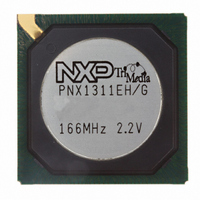
Manufacturer Part Number
PNX1311EH/G,557
Description
IC MEDIA PROC 166MHZ 292-HBGA
Manufacturer
NXP Semiconductors
Datasheet
1.PNX1300EHG557.pdf
(549 pages)
Specifications of PNX1311EH/G,557
Applications
Multimedia
Core Processor
TriMedia
Controller Series
Nexperia
Ram Size
48K x 8
Interface
I²C, 2-Wire Serial
Number Of I /o
169
Voltage - Supply
2.375 V ~ 2.625 V
Operating Temperature
0°C ~ 85°C
Mounting Type
Surface Mount
Package / Case
292-HBGA
Lead Free Status / RoHS Status
Lead free / RoHS Compliant
Program Memory Type
-
Other names
568-1295
935277721557
PNX1311EH/G
935277721557
PNX1311EH/G


PNX1300/01/02/11 Data Book
12.4
All devices must have a LVTTL, 3.3-V interface.
Table 12-2
in a 32-bit memory interface.
Table 12-2. Supported Rank Configurations (32-bit)
Refer to
evaluate the support of 2-bank, 64-Mbit devices. These
devices are not widely used. Hence they are not de-
scribed in this document.
Table 12-3
in a 16-bit memory interface.
Table 12-3. Supported Rank Configurations (16-bit)
12-2
Figure 12-1. PNX1300 internal highway bus to the external glueless SDRAM interface.
Device Size
Device Size
(Mbit)
(Mbit)
1. Limited support for a 32-MB configuration only.
2. However MM_CONFIG.SIZE may be set to
3. Limited support for a 64-MB configuration only.
4. However MM_CONFIG.SIZE is 32 MB (i.e. 7).
128
256
128
128
256
16
64
16
64
MEMORY DEVICES SUPPORTED
16MB (i.e. 6). Refer to
Figure 12-11
details.
1
3
Section 12.8, “Address Mapping,”
lists the devices and organizations supported
lists the devices and organizations supported
PNX1300
DSPCPU
Peripherals
On-Chip
2
4
2
4
4
4
4
4
4
4
2
2
4
512K
512K
512K
for the two possible connection
Device(s)
Device(s)
PRELIMINARY SPECIFICATION
1M 16 SDRAM
1M 32 SDRAM
2M 16 SDRAM
4M 16 SDRAM
1M 16 SDRAM
2M 16 SDRAM
4M 16 SDRAM
1M
2M
2M
Highway
PNX1300
Data
Interface
Memory
16 SDRAM
32 SDRAM
16 SDRAM
8 SDRAM
4 SDRAM
8 SDRAM
Figure 12-10
RAS#, CAS#, WE#
Byte Enables[3:0]
Clock Enables,
Chip Selects#
Rank Size
Rank Size
Data[31:0]
Address,
32
64
16
32
32
16 MB
16 MB
16 MB
4 MB
8 MB
8 MB
2 MB
8 MB
in order to
b
2
4
1
2
Clock
MB
MB
MB
MB
MB
and
33
12.4.1
PNX1300 supports synchronous DRAM chips directly.
SDRAM has a fast, synchronous interface that permits
burst transfers at 1 word per clock cycle. The memory in-
side an SDRAM device is divided into two or four banks;
the SDRAM implements interleaved bank access to sus-
tain maximum bandwidth.
SDRAM devices implement a power down mechanism
with self-refresh. PNX1300 power management takes
advantage of this mechanism.
PNX1300 supports only Jedec-compatible SDRAM with
two or four internal banks of memory per device.
12.4.2
Also supported in PNX1300 systems, SGRAM is essen-
tially an SDRAM with additional features for raster graph-
ics functions. The device type is standardized by Jedec
and offered by multiple DRAM vendors. Tying the DSF
input of an SGRAM low makes the device operates like
a standard 32-bit-wide SDRAM and thus compatible with
the PNX1300 memory interface. PNX1300 is not sup-
porting the new types of SGRAMs that have a DDR inter-
face.
12.5
PNX1300 supports a variety of memory sizes thanks to:
• Many possible configurations of SDRAM devices
• Support for up to four memory ranks
The minimum memory size is 4 MB using two
2 512K 16 SDRAM devices on the 32-bit data bus, or 2
MB with one of these devices on a 16-bit data bus. Up to
two memory devices can be connected without any glue
logic and without sacrificing performance. The maximum
memory size with full performance is 64MB using two
4 4M 16 SDRAM chips on a 32-bit data bus, and 32 MB
using one 4 4M 16 SDRAM chip on a 16-bit data bus.
Several memory configurations can be constructed using
more devices. To do so, the frequency of the memory in-
1.
2.
However MM_CONFIG.SIZE is set to 8 MB (i.e. 5)
However MM_CONFIG.SIZE is set to 8 MB (i.e. 5).
MEMORY GRANULARITY AND SIZES
SDRAM
SGRAM
CS#
Address, Control
DQM[3:0]
CLK
DQ[31:0]
Philips Semiconductors
SDRAM
Memory
Array
Related parts for PNX1311EH/G,557
Image
Part Number
Description
Manufacturer
Datasheet
Request
R

Part Number:
Description:
Manufacturer:
NXP Semiconductors
Datasheet:
Part Number:
Description:
Manufacturer:
NXP Semiconductors
Datasheet:

Part Number:
Description:
Video ICs NEXPERIA MEDIA PROCESSOR
Manufacturer:
NXP Semiconductors
Part Number:
Description:
NXP Semiconductors designed the LPC2420/2460 microcontroller around a 16-bit/32-bitARM7TDMI-S CPU core with real-time debug interfaces that include both JTAG andembedded trace
Manufacturer:
NXP Semiconductors
Datasheet:

Part Number:
Description:
NXP Semiconductors designed the LPC2458 microcontroller around a 16-bit/32-bitARM7TDMI-S CPU core with real-time debug interfaces that include both JTAG andembedded trace
Manufacturer:
NXP Semiconductors
Datasheet:
Part Number:
Description:
NXP Semiconductors designed the LPC2468 microcontroller around a 16-bit/32-bitARM7TDMI-S CPU core with real-time debug interfaces that include both JTAG andembedded trace
Manufacturer:
NXP Semiconductors
Datasheet:
Part Number:
Description:
NXP Semiconductors designed the LPC2470 microcontroller, powered by theARM7TDMI-S core, to be a highly integrated microcontroller for a wide range ofapplications that require advanced communications and high quality graphic displays
Manufacturer:
NXP Semiconductors
Datasheet:
Part Number:
Description:
NXP Semiconductors designed the LPC2478 microcontroller, powered by theARM7TDMI-S core, to be a highly integrated microcontroller for a wide range ofapplications that require advanced communications and high quality graphic displays
Manufacturer:
NXP Semiconductors
Datasheet:
Part Number:
Description:
The Philips Semiconductors XA (eXtended Architecture) family of 16-bit single-chip microcontrollers is powerful enough to easily handle the requirements of high performance embedded applications, yet inexpensive enough to compete in the market for hi
Manufacturer:
NXP Semiconductors
Datasheet:
Part Number:
Description:
The XA-S3 device is a member of Philips Semiconductors? XA(eXtended Architecture) family of high performance 16-bitsingle-chip microcontrollers
Manufacturer:
NXP Semiconductors
Datasheet:

Part Number:
Description:
The NXP BlueStreak LH75401/LH75411 family consists of two low-cost 16/32-bit System-on-Chip (SoC) devices
Manufacturer:
NXP Semiconductors
Datasheet:
Part Number:
Description:
The NXP LPC3130/3131 combine an 180 MHz ARM926EJ-S CPU core, high-speed USB2
Manufacturer:
NXP Semiconductors
Datasheet:
Part Number:
Description:
The NXP LPC3141 combine a 270 MHz ARM926EJ-S CPU core, High-speed USB 2
Manufacturer:
NXP Semiconductors
Part Number:
Description:
The NXP LPC3143 combine a 270 MHz ARM926EJ-S CPU core, High-speed USB 2
Manufacturer:
NXP Semiconductors