PNX1311EH/G,557 NXP Semiconductors, PNX1311EH/G,557 Datasheet - Page 209
PNX1311EH/G,557
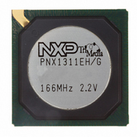
Manufacturer Part Number
PNX1311EH/G,557
Description
IC MEDIA PROC 166MHZ 292-HBGA
Manufacturer
NXP Semiconductors
Datasheet
1.PNX1300EHG557.pdf
(549 pages)
Specifications of PNX1311EH/G,557
Applications
Multimedia
Core Processor
TriMedia
Controller Series
Nexperia
Ram Size
48K x 8
Interface
I²C, 2-Wire Serial
Number Of I /o
169
Voltage - Supply
2.375 V ~ 2.625 V
Operating Temperature
0°C ~ 85°C
Mounting Type
Surface Mount
Package / Case
292-HBGA
Lead Free Status / RoHS Status
Lead free / RoHS Compliant
Program Memory Type
-
Other names
568-1295
935277721557
PNX1311EH/G
935277721557
PNX1311EH/G


Philips Semiconductors
13.5
Figure 13-3
for three types of read accesses supported by I
EEPROMs. A read from the address currently latched in-
side the EEPROM can be for either a single byte or for
an arbitrary series of sequential bytes. The master
makes the choice by setting the ACK bit after a byte has
been transferred.
Figure 13-3. Protocols supported by the boot block for reading the EEPROM
EEPROM ACCESS PROTOCOLS
Current-Address Read
SDA Line Protocol:
SDA Line Protocol:
SDA Line Protocol:
shows the SDA (serial data) line protocols
Sequential Read
Random Read
S
T
A
R
T
S
T
A
R
T
S
T
A
R
T
1 0 1 0
1 0 1 0
Device Address
Device Address
1 0 1 0
Device Address
D
A
A
0
0
Dummy Write
A
P
A
P
0
0
0
P
0
P
A
0
P
0
W
P
R
E
R
E
A
D
0
T
I
R
E
A
D
A
C
K
A
C
K
W
A
C
K
A
7
D
7
W
2
D
7
A
6
D
6
C serial
W
D
A
D
6
5
5
Data n
W
D
5
A
4
D
4
Data n
W
D
4
A
3
D
3
W
D
A
D
3
2
2
W
D
A
D
2
1
1
W
D
1
A
0
D
0
D
0
A
C
K
A
C
K
N
O
A
C
K
S
A
R
D
A random-access read is accomplished by performing a
dummy write, which overwrites the latched address
stored inside the EEPROM. Once the internal address
latch is set to the desired value, one of the other two read
protocols can be used to read one or more bytes.
The boot logic inside PNX1300 uses a single random
read transaction to location 0 of device address 1010000
followed by a sequential read extension to read all re-
quired EEPROM bytes in a single pass.
T
T
7
PRELIMINARY SPECIFICATION
O
S
T
P
1 0 1 0
D
6
Device Address
Data n+1
D
5
D
4
D
3
A
0
D
2
P
D
1
1
P
D
0
0
R
E
A
D
A
C
K
A
C
K
D
7
D
D
7
6
Data n+2
D
D
6
5
D
5
D
4
D
D
4
3
D
D
3
2
D
2
D
1
D
1
D
0
D
A
C
K
0
O
N
A
C
K
D
7
O
S
T
P
D
6
Data n+3
D
5
D
4
D
3
D
2
System Boot
D
1
D
0
O
N
A
C
K
S
O
P
T
13-9
Related parts for PNX1311EH/G,557
Image
Part Number
Description
Manufacturer
Datasheet
Request
R

Part Number:
Description:
Manufacturer:
NXP Semiconductors
Datasheet:
Part Number:
Description:
Manufacturer:
NXP Semiconductors
Datasheet:

Part Number:
Description:
Video ICs NEXPERIA MEDIA PROCESSOR
Manufacturer:
NXP Semiconductors
Part Number:
Description:
NXP Semiconductors designed the LPC2420/2460 microcontroller around a 16-bit/32-bitARM7TDMI-S CPU core with real-time debug interfaces that include both JTAG andembedded trace
Manufacturer:
NXP Semiconductors
Datasheet:

Part Number:
Description:
NXP Semiconductors designed the LPC2458 microcontroller around a 16-bit/32-bitARM7TDMI-S CPU core with real-time debug interfaces that include both JTAG andembedded trace
Manufacturer:
NXP Semiconductors
Datasheet:
Part Number:
Description:
NXP Semiconductors designed the LPC2468 microcontroller around a 16-bit/32-bitARM7TDMI-S CPU core with real-time debug interfaces that include both JTAG andembedded trace
Manufacturer:
NXP Semiconductors
Datasheet:
Part Number:
Description:
NXP Semiconductors designed the LPC2470 microcontroller, powered by theARM7TDMI-S core, to be a highly integrated microcontroller for a wide range ofapplications that require advanced communications and high quality graphic displays
Manufacturer:
NXP Semiconductors
Datasheet:
Part Number:
Description:
NXP Semiconductors designed the LPC2478 microcontroller, powered by theARM7TDMI-S core, to be a highly integrated microcontroller for a wide range ofapplications that require advanced communications and high quality graphic displays
Manufacturer:
NXP Semiconductors
Datasheet:
Part Number:
Description:
The Philips Semiconductors XA (eXtended Architecture) family of 16-bit single-chip microcontrollers is powerful enough to easily handle the requirements of high performance embedded applications, yet inexpensive enough to compete in the market for hi
Manufacturer:
NXP Semiconductors
Datasheet:
Part Number:
Description:
The XA-S3 device is a member of Philips Semiconductors? XA(eXtended Architecture) family of high performance 16-bitsingle-chip microcontrollers
Manufacturer:
NXP Semiconductors
Datasheet:

Part Number:
Description:
The NXP BlueStreak LH75401/LH75411 family consists of two low-cost 16/32-bit System-on-Chip (SoC) devices
Manufacturer:
NXP Semiconductors
Datasheet:
Part Number:
Description:
The NXP LPC3130/3131 combine an 180 MHz ARM926EJ-S CPU core, high-speed USB2
Manufacturer:
NXP Semiconductors
Datasheet:
Part Number:
Description:
The NXP LPC3141 combine a 270 MHz ARM926EJ-S CPU core, High-speed USB 2
Manufacturer:
NXP Semiconductors
Part Number:
Description:
The NXP LPC3143 combine a 270 MHz ARM926EJ-S CPU core, High-speed USB 2
Manufacturer:
NXP Semiconductors