PNX1311EH/G,557 NXP Semiconductors, PNX1311EH/G,557 Datasheet - Page 242
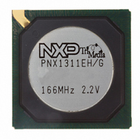
PNX1311EH/G,557
Manufacturer Part Number
PNX1311EH/G,557
Description
IC MEDIA PROC 166MHZ 292-HBGA
Manufacturer
NXP Semiconductors
Datasheet
1.PNX1300EHG557.pdf
(549 pages)
Specifications of PNX1311EH/G,557
Applications
Multimedia
Core Processor
TriMedia
Controller Series
Nexperia
Ram Size
48K x 8
Interface
I²C, 2-Wire Serial
Number Of I /o
169
Voltage - Supply
2.375 V ~ 2.625 V
Operating Temperature
0°C ~ 85°C
Mounting Type
Surface Mount
Package / Case
292-HBGA
Lead Free Status / RoHS Status
Lead free / RoHS Compliant
Program Memory Type
-
Other names
568-1295
935277721557
PNX1311EH/G
935277721557
PNX1311EH/G


PNX1300/01/02/11 Data Book
15.5.2
The DCT coefficients associated with the macroblock are
output to a separate memory area and each DCT coeffi-
cient is represented as one 32-bit quantity (16 bits of run
and 16 bits of level). For intra blocks, the DC term is ex-
pressed as 16 bits of DC size and a 16-bit value whose
most significant bits (the number of bits used for DC level
is determined by DC size) represent the DC level. Each
block of DCT coefficients is terminated by a run value of
‘0xff’.
15.6
The PNX1300 VLD is targeted for a single bitstream de-
code and there is no provision to decode more than one
bitstream at a time by using the VLD in time multiplexed
mode. However internal development has shown that up
to 4 simultaneous MPEG1 bitstreams can be decoded.
This procedure is beyond the scope of this databook but
can be discussed further by contacting customer sup-
port.
15.7
To ensure compatibility with future devices, any unde-
fined MMIO bits should be ignored when read, and writ-
ten as ‘0’s.
15-4
Figure 15-3. MPEG1 Macroblock Header Output Format
First Forward Motion Vector
31
First Backward Motion Vector
31
31
31
VLD TIME SHARING
MMIO REGISTERS
Run-Level Output Data
30
30
25
Esc Count
PRELIMINARY SPECIFICATION
Motion Code [0][0][0]
Motion Code [0][1][0]
29
29
17
MBA Inc
Motion Residual [0][0][0]
23
Motion Residual [0][1][0]
23
11
MB Type
6
15.7.1
This register contains the current status information most
pertinent to the normal operation of an MPEG video de-
code application. VLD status description is detailed in
Table 15-3
ter hardware reset) is ‘0’.
Interrupts can be enabled for any of the defined status
bits (see following VLD_IMASK description). Acknowl-
edgment of the interrupt is done by writing a ‘1’ to the cor-
responding bit in VLD_STATUS register. Writing a one to
the bits one through five clears the corresponding bits.
However bit 0 (COMMAND_DONE) is cleared only by is-
suing a new command. Writing a ‘0’ to bit 0 of the status
register will result in undefined behavior of the VLD. Note
that several status bits may be asserted simultaneously.
Thus it is recommended to use level triggered interrupts
(see
knowledge the interrupt.
15.7.2
This register allows the DSPCPU to control the initiation
of the interrupt for the corresponding bits in the VLD Sta-
tus Register. Writing a ‘1’ into any of the defined
VLD_IMASK bits enables the interrupt for the corre-
sponding bit in the status register (VLD_STATUS). De-
fault value (after hardware reset) is ‘0’.
15
15
4
Section 3.5.3.6 on page
Motion Code [0][0][1]
VLD Status (VLD_STATUS)
VLD Interrupt Enable (VLD_IMASK)
Motion Code [0][1][1]
13
13
and pictured in
3
14
12
2
Figure
Philips Semiconductors
7
7
10
Motion Residual [0][0][1]
Motion Residual [0][1][1]
3-11) and carefully ac-
CBP
15-4. Default value (af-
1
quant scale
4
0
w0
w1
w2
w3
Related parts for PNX1311EH/G,557
Image
Part Number
Description
Manufacturer
Datasheet
Request
R

Part Number:
Description:
Manufacturer:
NXP Semiconductors
Datasheet:
Part Number:
Description:
Manufacturer:
NXP Semiconductors
Datasheet:

Part Number:
Description:
Video ICs NEXPERIA MEDIA PROCESSOR
Manufacturer:
NXP Semiconductors
Part Number:
Description:
NXP Semiconductors designed the LPC2420/2460 microcontroller around a 16-bit/32-bitARM7TDMI-S CPU core with real-time debug interfaces that include both JTAG andembedded trace
Manufacturer:
NXP Semiconductors
Datasheet:

Part Number:
Description:
NXP Semiconductors designed the LPC2458 microcontroller around a 16-bit/32-bitARM7TDMI-S CPU core with real-time debug interfaces that include both JTAG andembedded trace
Manufacturer:
NXP Semiconductors
Datasheet:
Part Number:
Description:
NXP Semiconductors designed the LPC2468 microcontroller around a 16-bit/32-bitARM7TDMI-S CPU core with real-time debug interfaces that include both JTAG andembedded trace
Manufacturer:
NXP Semiconductors
Datasheet:
Part Number:
Description:
NXP Semiconductors designed the LPC2470 microcontroller, powered by theARM7TDMI-S core, to be a highly integrated microcontroller for a wide range ofapplications that require advanced communications and high quality graphic displays
Manufacturer:
NXP Semiconductors
Datasheet:
Part Number:
Description:
NXP Semiconductors designed the LPC2478 microcontroller, powered by theARM7TDMI-S core, to be a highly integrated microcontroller for a wide range ofapplications that require advanced communications and high quality graphic displays
Manufacturer:
NXP Semiconductors
Datasheet:
Part Number:
Description:
The Philips Semiconductors XA (eXtended Architecture) family of 16-bit single-chip microcontrollers is powerful enough to easily handle the requirements of high performance embedded applications, yet inexpensive enough to compete in the market for hi
Manufacturer:
NXP Semiconductors
Datasheet:
Part Number:
Description:
The XA-S3 device is a member of Philips Semiconductors? XA(eXtended Architecture) family of high performance 16-bitsingle-chip microcontrollers
Manufacturer:
NXP Semiconductors
Datasheet:

Part Number:
Description:
The NXP BlueStreak LH75401/LH75411 family consists of two low-cost 16/32-bit System-on-Chip (SoC) devices
Manufacturer:
NXP Semiconductors
Datasheet:
Part Number:
Description:
The NXP LPC3130/3131 combine an 180 MHz ARM926EJ-S CPU core, high-speed USB2
Manufacturer:
NXP Semiconductors
Datasheet:
Part Number:
Description:
The NXP LPC3141 combine a 270 MHz ARM926EJ-S CPU core, High-speed USB 2
Manufacturer:
NXP Semiconductors
Part Number:
Description:
The NXP LPC3143 combine a 270 MHz ARM926EJ-S CPU core, High-speed USB 2
Manufacturer:
NXP Semiconductors