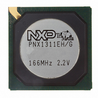
PNX1311EH/G,557 NXP Semiconductors, PNX1311EH/G,557 Datasheet - Page 520

PNX1311EH/G,557
Manufacturer Part Number
PNX1311EH/G,557
Description
IC MEDIA PROC 166MHZ 292-HBGA
Manufacturer
NXP Semiconductors
Datasheet
1.PNX1300EHG557.pdf
(549 pages)
Specifications of PNX1311EH/G,557
Applications
Multimedia
Core Processor
TriMedia
Controller Series
Nexperia
Ram Size
48K x 8
Interface
I²C, 2-Wire Serial
Number Of I /o
169
Voltage - Supply
2.375 V ~ 2.625 V
Operating Temperature
0°C ~ 85°C
Mounting Type
Surface Mount
Package / Case
292-HBGA
Lead Free Status / RoHS Status
Lead free / RoHS Compliant
Program Memory Type
-
Other names
568-1295
935277721557
PNX1311EH/G
935277721557
PNX1311EH/G
- Current page: 520 of 549
- Download datasheet (6Mb)
PNX1300/01/02/11 Data Book
C-4
Figure C-3. Byte mask, planar YUV 4:2:0 and YUV 4:2:2 for ICP, VO or VI memory data in Little and Big En-
dian modes
Figure C-4. RBG-24+ data format for ICP in Little and Big Endian modes
Figure C-5. RBG-15+ data format for ICP in Little and Big Endian modes
Y pixel byte data
in memory
(same for U, V, B)
Pixel half-word data
in memory or PCI
Pixel word data
in memory or PCI
PRELIMINARY SPECIFICATION
31
31
31
A+3
Y3
A+3
G1B1
G3B3
Y7
B0
B1
A+3
Big Endian Mode
Big Endian Mode
P
n+1
A+2
Big Endian Mode
A+2
R1G’1
Y2
Y6
G0
G1
R3G’3
A+2
A+1
A+1
G0B0
G2B2
Y1
Y5
A+1
R0
R1
Note: A+0 corresponds to byte-0 lane of SDRAM/Hwy/PCI
and A+3 corresponds to byte-3 lane of SDRAM/Hwy/PCI
Note: A+0 corresponds to byte-0 lane of SDRAM/Hwy/PCI
and A+3 corresponds to byte-3 lane of SDRAM/Hwy/PCI
P
Note: A+0 corresponds to byte-0 lane of SDRAM/Hwy
and A+3 corresponds to byte-3 lane of SDRAM/Hwy
n
A+0
A+0
Y0
Y4
R2G’2
A+0
R0G’0
0
1
0
0
0
31
31
31
A+3
Y3
Y7
A+3
Little Endian Mode
R3G’3
R1G’1
A+3
Little Endian Mode
0
1
P
Little Endian Mode
n+1
A+2
A+2
Y2
Y6
G1B1
G3B3
A+2
R0
R1
Philips Semiconductors
A+1
A+1
Y1
Y5
A+1
R2G’2
G0
G1
R0G’0
P
n
A+0
A+0
Y0
Y4
G0B0
G2B2
A+0
B0
B1
0
0
0
Related parts for PNX1311EH/G,557
Image
Part Number
Description
Manufacturer
Datasheet
Request
R

Part Number:
Description:
Manufacturer:
NXP Semiconductors
Datasheet:

Part Number:
Description:
Manufacturer:
NXP Semiconductors
Datasheet:
Part Number:
Description:
Video ICs NEXPERIA MEDIA PROCESSOR
Manufacturer:
NXP Semiconductors
Part Number:
Description:
NXP Semiconductors designed the LPC2420/2460 microcontroller around a 16-bit/32-bitARM7TDMI-S CPU core with real-time debug interfaces that include both JTAG andembedded trace
Manufacturer:
NXP Semiconductors
Datasheet:

Part Number:
Description:
NXP Semiconductors designed the LPC2458 microcontroller around a 16-bit/32-bitARM7TDMI-S CPU core with real-time debug interfaces that include both JTAG andembedded trace
Manufacturer:
NXP Semiconductors
Datasheet:
Part Number:
Description:
NXP Semiconductors designed the LPC2468 microcontroller around a 16-bit/32-bitARM7TDMI-S CPU core with real-time debug interfaces that include both JTAG andembedded trace
Manufacturer:
NXP Semiconductors
Datasheet:
Part Number:
Description:
NXP Semiconductors designed the LPC2470 microcontroller, powered by theARM7TDMI-S core, to be a highly integrated microcontroller for a wide range ofapplications that require advanced communications and high quality graphic displays
Manufacturer:
NXP Semiconductors
Datasheet:
Part Number:
Description:
NXP Semiconductors designed the LPC2478 microcontroller, powered by theARM7TDMI-S core, to be a highly integrated microcontroller for a wide range ofapplications that require advanced communications and high quality graphic displays
Manufacturer:
NXP Semiconductors
Datasheet:
Part Number:
Description:
The Philips Semiconductors XA (eXtended Architecture) family of 16-bit single-chip microcontrollers is powerful enough to easily handle the requirements of high performance embedded applications, yet inexpensive enough to compete in the market for hi
Manufacturer:
NXP Semiconductors
Datasheet:
Part Number:
Description:
The XA-S3 device is a member of Philips Semiconductors? XA(eXtended Architecture) family of high performance 16-bitsingle-chip microcontrollers
Manufacturer:
NXP Semiconductors
Datasheet:

Part Number:
Description:
The NXP BlueStreak LH75401/LH75411 family consists of two low-cost 16/32-bit System-on-Chip (SoC) devices
Manufacturer:
NXP Semiconductors
Datasheet:

Part Number:
Description:
The NXP LPC3130/3131 combine an 180 MHz ARM926EJ-S CPU core, high-speed USB2
Manufacturer:
NXP Semiconductors
Datasheet:

Part Number:
Description:
The NXP LPC3141 combine a 270 MHz ARM926EJ-S CPU core, High-speed USB 2
Manufacturer:
NXP Semiconductors

Part Number:
Description:
The NXP LPC3143 combine a 270 MHz ARM926EJ-S CPU core, High-speed USB 2
Manufacturer:
NXP Semiconductors


