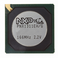
PNX1311EH/G,557 NXP Semiconductors, PNX1311EH/G,557 Datasheet - Page 45

PNX1311EH/G,557
Manufacturer Part Number
PNX1311EH/G,557
Description
IC MEDIA PROC 166MHZ 292-HBGA
Manufacturer
NXP Semiconductors
Datasheet
1.PNX1300EHG557.pdf
(549 pages)
Specifications of PNX1311EH/G,557
Applications
Multimedia
Core Processor
TriMedia
Controller Series
Nexperia
Ram Size
48K x 8
Interface
I²C, 2-Wire Serial
Number Of I /o
169
Voltage - Supply
2.375 V ~ 2.625 V
Operating Temperature
0°C ~ 85°C
Mounting Type
Surface Mount
Package / Case
292-HBGA
Lead Free Status / RoHS Status
Lead free / RoHS Compliant
Program Memory Type
-
Other names
568-1295
935277721557
PNX1311EH/G
935277721557
PNX1311EH/G
- Current page: 45 of 549
- Download datasheet (6Mb)
Philips Semiconductors
1.9.7.12
Notes: 1. See the timing measurement conditions in
1.9.7.13
Notes: 1. See the timing measurement conditions in
1.9.7.14
Notes: 1. See the timing measurement conditions in
1.9.7.15
Notes: 1. See the timing measurement conditions in
f
T
T
T
f
T
T
T
T
T
T
T
T
T
T
f
T
T
f
T
T
T
T
JTAG-CLK
SCL
VI-CLK
VO-CLK
clk-TDO
su-TCK
h-TCK
BUF
su-STA
h-STA
LOW
HIGH
f
su-SDA
h-SDA
dv-SDA
dv-STO
su-CLK
h-CLK
CLK-DV
CLK-DV
su-CLK
h-CLK
Symbol
Symbol
Symbol
Symbol
2. See the timing measurement conditions in
2. See the timing measurement conditions in
3. See the timing measurement conditions in
4. See the timing measurement conditions in
5. See the timing measurement conditions in
2. See the timing measurement conditions in
3. CLKOUT asserted, i.e. the VO unit is the source of VO_CLK
4. CLKOUT negated, i.e. the external world is the source of VO_CLK
JTAG I/O timing
I
Video In I/O Timing
Video Out I/O Timing
2
C I/O timing
JTAG clock frequency
JTAG_TCK to JTAG_TDO valid delay
Input setup time to JTAG_TCK
Input hold time from JTAG_TCK
SCL clock frequency
Bus free time
Start condition set up time
Start condition hold time
SCL LOW time
SCL HIGH time
SCL and SDA fall time (Cb = 10-400 pF, from V
Data setup time
Data hold time
SCL LOW to data out valid
SCL HIGH to data out
Video In clock frequency
Input setup time to VI_CLK
Input hold time from VI_CLK
Video Out clock frequency
VO_CLK to VO_DATA (or VO_IO*) out
VO_CLK to VO_DATA (or VO_IO*) out
VO_IO* setup time to VO_CLK
VO_IO* hold time from VO_CLK
Parameter
Parameter
Parameter
Parameter
Figure
Figure
Figure
Figure
Figure
Figure
Figure
Figure
Figure
Figure
1-10.
1-9.
1-11.
1-12.
1-13.
1-14.
1-15.
1-16.
1-17.
1-18.
IH-IIC
PRELIMINARY SPECIFICATION
to V
IL-IIC
Min.
Min.
Min.
10
)
2
2
2
3
7
3
3
3
20+0.1Cb
Min.
Max
Max
100
Max
7.5
7.5
81
81
20
10
1
1
1
1
1
0
1
Units
Units
Units
MHz
MHz
MHz
Max
400
250
0.5
ns
ns
ns
ns
ns
ns
ns
ns
ns
Notes
Notes
Notes
Units
kHz
1,3
1,4
ns
ns
ns
ns
1
1
1
2
2
2
2
s
s
s
s
s
s
Pin List
Notes
1
2
3
3
1
1
1
4
4
5
5
1-19
Related parts for PNX1311EH/G,557
Image
Part Number
Description
Manufacturer
Datasheet
Request
R

Part Number:
Description:
Manufacturer:
NXP Semiconductors
Datasheet:

Part Number:
Description:
Manufacturer:
NXP Semiconductors
Datasheet:
Part Number:
Description:
Video ICs NEXPERIA MEDIA PROCESSOR
Manufacturer:
NXP Semiconductors
Part Number:
Description:
NXP Semiconductors designed the LPC2420/2460 microcontroller around a 16-bit/32-bitARM7TDMI-S CPU core with real-time debug interfaces that include both JTAG andembedded trace
Manufacturer:
NXP Semiconductors
Datasheet:

Part Number:
Description:
NXP Semiconductors designed the LPC2458 microcontroller around a 16-bit/32-bitARM7TDMI-S CPU core with real-time debug interfaces that include both JTAG andembedded trace
Manufacturer:
NXP Semiconductors
Datasheet:
Part Number:
Description:
NXP Semiconductors designed the LPC2468 microcontroller around a 16-bit/32-bitARM7TDMI-S CPU core with real-time debug interfaces that include both JTAG andembedded trace
Manufacturer:
NXP Semiconductors
Datasheet:
Part Number:
Description:
NXP Semiconductors designed the LPC2470 microcontroller, powered by theARM7TDMI-S core, to be a highly integrated microcontroller for a wide range ofapplications that require advanced communications and high quality graphic displays
Manufacturer:
NXP Semiconductors
Datasheet:
Part Number:
Description:
NXP Semiconductors designed the LPC2478 microcontroller, powered by theARM7TDMI-S core, to be a highly integrated microcontroller for a wide range ofapplications that require advanced communications and high quality graphic displays
Manufacturer:
NXP Semiconductors
Datasheet:
Part Number:
Description:
The Philips Semiconductors XA (eXtended Architecture) family of 16-bit single-chip microcontrollers is powerful enough to easily handle the requirements of high performance embedded applications, yet inexpensive enough to compete in the market for hi
Manufacturer:
NXP Semiconductors
Datasheet:
Part Number:
Description:
The XA-S3 device is a member of Philips Semiconductors? XA(eXtended Architecture) family of high performance 16-bitsingle-chip microcontrollers
Manufacturer:
NXP Semiconductors
Datasheet:

Part Number:
Description:
The NXP BlueStreak LH75401/LH75411 family consists of two low-cost 16/32-bit System-on-Chip (SoC) devices
Manufacturer:
NXP Semiconductors
Datasheet:

Part Number:
Description:
The NXP LPC3130/3131 combine an 180 MHz ARM926EJ-S CPU core, high-speed USB2
Manufacturer:
NXP Semiconductors
Datasheet:

Part Number:
Description:
The NXP LPC3141 combine a 270 MHz ARM926EJ-S CPU core, High-speed USB 2
Manufacturer:
NXP Semiconductors

Part Number:
Description:
The NXP LPC3143 combine a 270 MHz ARM926EJ-S CPU core, High-speed USB 2
Manufacturer:
NXP Semiconductors


