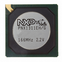
PNX1311EH/G,557 NXP Semiconductors, PNX1311EH/G,557 Datasheet - Page 256

PNX1311EH/G,557
Manufacturer Part Number
PNX1311EH/G,557
Description
IC MEDIA PROC 166MHZ 292-HBGA
Manufacturer
NXP Semiconductors
Datasheet
1.PNX1300EHG557.pdf
(549 pages)
Specifications of PNX1311EH/G,557
Applications
Multimedia
Core Processor
TriMedia
Controller Series
Nexperia
Ram Size
48K x 8
Interface
I²C, 2-Wire Serial
Number Of I /o
169
Voltage - Supply
2.375 V ~ 2.625 V
Operating Temperature
0°C ~ 85°C
Mounting Type
Surface Mount
Package / Case
292-HBGA
Lead Free Status / RoHS Status
Lead free / RoHS Compliant
Program Memory Type
-
Other names
568-1295
935277721557
PNX1311EH/G
935277721557
PNX1311EH/G
- Current page: 256 of 549
- Download datasheet (6Mb)
PNX1300/01/02/11 Data Book
17.3.1
Figure 17-2
purpose I/O pins. The SSI_IO1 and SSI_IO2 external
pins may be used as general purpose I/O by proper con-
figuration of the SSI_CTL register, or they may be used
as transmit clock input and as transmit framing signal in-
put or output. The SSI_CTL.IO1 and SSI_CTL.IO2 Mode
Select fields control the direction and functionality of
these two pins.
17-2
Figure 17-1. The SSI interface block diagram
Figure 17-2. I/O block diagram
SSI_RxDATA
SSI_RxCLK
SSI_RxFSX
SSI_IO1
SSI_IO1
SSI_IO2
General Purpose I/O
internal TxFSX
SSI_RxFSX
illustrates the functionality of the general
SSI_IO2
PRELIMINARY SPECIFICATION
IO1[1:0]=00
IO1[1:0]=01
IO2[1:0] = 10
IO2[1:0] = 10
internal TxFSX
Frame Synchronization
SSI Receive
WIO2
I/O Control
Block
Block
Block
MUX
2:1
WIO1
RIO1
IO2[1:0] = 00
IO2[1:0] = 00
IO2[1:0] = 11
IO2[1:0] = 11
SSI_RxCLK
TxCLK
TxFSX
SSI_IO1
A hardware reset or a software reset of the transmitter
through SSI_CTL.TXR command sets the SSI_CTL.IO1
and SSI_CTL.O2 fields to 11b, a conflict-free initial pin
state.Table 17-2
SSI_IO1,
on SSI_IO2. Note: If SSI_IO1 is not selected as transmit
clock input, the transmit clock is taken from the receive
clock signal instead. If SSI_IO2 is not selected as trans-
mit framing signal input or output, the transmit framing
signal is taken from the receive framing signal instead.
MUX
MUX
2:1
2:1
SSI Transmit
Table 17-3
IO1[1:0]=10
IO1[1:0]=10
Block
IO2[0] = 0
shows the effect of SSI_CTL.IO1 on pin
TxFSX
shows the effect of SSI_CTL.IO2
MUX
2:1
Philips Semiconductors
TxCLK
IO2[0] = 1
SSI_TxDATA
RIO2
SSI_IO2
Related parts for PNX1311EH/G,557
Image
Part Number
Description
Manufacturer
Datasheet
Request
R

Part Number:
Description:
Manufacturer:
NXP Semiconductors
Datasheet:

Part Number:
Description:
Manufacturer:
NXP Semiconductors
Datasheet:
Part Number:
Description:
Video ICs NEXPERIA MEDIA PROCESSOR
Manufacturer:
NXP Semiconductors
Part Number:
Description:
NXP Semiconductors designed the LPC2420/2460 microcontroller around a 16-bit/32-bitARM7TDMI-S CPU core with real-time debug interfaces that include both JTAG andembedded trace
Manufacturer:
NXP Semiconductors
Datasheet:

Part Number:
Description:
NXP Semiconductors designed the LPC2458 microcontroller around a 16-bit/32-bitARM7TDMI-S CPU core with real-time debug interfaces that include both JTAG andembedded trace
Manufacturer:
NXP Semiconductors
Datasheet:
Part Number:
Description:
NXP Semiconductors designed the LPC2468 microcontroller around a 16-bit/32-bitARM7TDMI-S CPU core with real-time debug interfaces that include both JTAG andembedded trace
Manufacturer:
NXP Semiconductors
Datasheet:
Part Number:
Description:
NXP Semiconductors designed the LPC2470 microcontroller, powered by theARM7TDMI-S core, to be a highly integrated microcontroller for a wide range ofapplications that require advanced communications and high quality graphic displays
Manufacturer:
NXP Semiconductors
Datasheet:
Part Number:
Description:
NXP Semiconductors designed the LPC2478 microcontroller, powered by theARM7TDMI-S core, to be a highly integrated microcontroller for a wide range ofapplications that require advanced communications and high quality graphic displays
Manufacturer:
NXP Semiconductors
Datasheet:
Part Number:
Description:
The Philips Semiconductors XA (eXtended Architecture) family of 16-bit single-chip microcontrollers is powerful enough to easily handle the requirements of high performance embedded applications, yet inexpensive enough to compete in the market for hi
Manufacturer:
NXP Semiconductors
Datasheet:
Part Number:
Description:
The XA-S3 device is a member of Philips Semiconductors? XA(eXtended Architecture) family of high performance 16-bitsingle-chip microcontrollers
Manufacturer:
NXP Semiconductors
Datasheet:

Part Number:
Description:
The NXP BlueStreak LH75401/LH75411 family consists of two low-cost 16/32-bit System-on-Chip (SoC) devices
Manufacturer:
NXP Semiconductors
Datasheet:

Part Number:
Description:
The NXP LPC3130/3131 combine an 180 MHz ARM926EJ-S CPU core, high-speed USB2
Manufacturer:
NXP Semiconductors
Datasheet:

Part Number:
Description:
The NXP LPC3141 combine a 270 MHz ARM926EJ-S CPU core, High-speed USB 2
Manufacturer:
NXP Semiconductors

Part Number:
Description:
The NXP LPC3143 combine a 270 MHz ARM926EJ-S CPU core, High-speed USB 2
Manufacturer:
NXP Semiconductors


