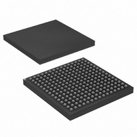
AT91CAP7E-NA-ZJ Atmel, AT91CAP7E-NA-ZJ Datasheet - Page 127

AT91CAP7E-NA-ZJ
Manufacturer Part Number
AT91CAP7E-NA-ZJ
Description
MCU CAP7 FPGA 225LFBGA
Manufacturer
Atmel
Series
CAP™r
Specifications of AT91CAP7E-NA-ZJ
Core Processor
ARM7
Core Size
16/32-Bit
Speed
80MHz
Connectivity
EBI/EMI, FPGA, IrDA, SPI, UART/USART, USB
Peripherals
DMA, POR, PWM, WDT
Number Of I /o
32
Program Memory Size
256KB (256K x 8)
Program Memory Type
ROM
Ram Size
160K x 8
Voltage - Supply (vcc/vdd)
1.08 V ~ 1.32 V
Data Converters
A/D 8x10b
Oscillator Type
Internal
Operating Temperature
-40°C ~ 85°C
Package / Case
225-LFBGA
Processor Series
AT91Mx
Core
ARM7TDMI
Data Bus Width
32 bit
3rd Party Development Tools
JTRACE-ARM-2M, MDK-ARM, RL-ARM, ULINK2
Lead Free Status / RoHS Status
Lead free / RoHS Compliant
Eeprom Size
-
Lead Free Status / Rohs Status
Details
Available stocks
Company
Part Number
Manufacturer
Quantity
Price
- Current page: 127 of 520
- Download datasheet (11Mb)
20.6.6
8549A–CAP–10/08
NAND Flash Support
Figure 20-5. CompactFlash Application Example
The EBI integrates circuitry that interfaces to NAND Flash devices.
The NAND Flash logic is driven by the Static Memory Controller on the NCS3 address space.
Programming the CS3A field in the CSA Register in the Bus Matrix User Interface to the appro-
priate value enables the NAND Flash logic. For details on this register, refer to the Bus Matrix
User Interface section. Access to an external NAND Flash device is then made by accessing the
address space reserved to NCS3 (i.e., between 0x40000000 and 0x4FFF FFFF).
The NAND Flash Logic drives the read and write command signals of the SMC on the NANDOE
and NANDWE signals when the NCS3 signal is active. NANDOE and NANDWE are invalidated
as soon as the transfer address fails to lie in the NCS3 address space. For details on these
waveforms, refer to the Static Memory Controller section.
The NANDOE and NANDWE signals are multiplexed with NCS6 and NCS7 signals of the Static
Memory Controller. This multiplexing is controlled in the MUX logic part of the EBI by the CS3A
bit in the in the CSA Register For details on this register, refer to the Bus Matrix User Interface
Section. NCS6 and NCS7 become unavailable. Performing an access within the address space
reserved to NCS6 and NCS7 (i.e., between 0x70000000 and 0x8FFF FFFF) may lead to an
unpredictable outcome.
NWR1/CFIOR
NWR3/CFIOW
NCS4/CFCS0
A25/CFRNW
NWE/CFWE
EBI
NRD/CFOE
A22/REG
CD (PIO)
D[15:0]
NWAIT
CFCE1
CFCE2
A[10:0]
DIR
/OE
/OE
CompactFlash Connector
AT91CAP7E
D[15:0]
_CD1
_CD2
A[10:0]
_REG
_OE
_WE
_IORD
_IOWR
_CE1
_CE2
_WAIT
127
Related parts for AT91CAP7E-NA-ZJ
Image
Part Number
Description
Manufacturer
Datasheet
Request
R

Part Number:
Description:
Customizable Microcontroller
Manufacturer:
ATMEL Corporation
Datasheet:

Part Number:
Description:
DEV KIT FOR AVR/AVR32
Manufacturer:
Atmel
Datasheet:

Part Number:
Description:
INTERVAL AND WIPE/WASH WIPER CONTROL IC WITH DELAY
Manufacturer:
ATMEL Corporation
Datasheet:

Part Number:
Description:
Low-Voltage Voice-Switched IC for Hands-Free Operation
Manufacturer:
ATMEL Corporation
Datasheet:

Part Number:
Description:
MONOLITHIC INTEGRATED FEATUREPHONE CIRCUIT
Manufacturer:
ATMEL Corporation
Datasheet:

Part Number:
Description:
AM-FM Receiver IC U4255BM-M
Manufacturer:
ATMEL Corporation
Datasheet:

Part Number:
Description:
Monolithic Integrated Feature Phone Circuit
Manufacturer:
ATMEL Corporation
Datasheet:

Part Number:
Description:
Multistandard Video-IF and Quasi Parallel Sound Processing
Manufacturer:
ATMEL Corporation
Datasheet:

Part Number:
Description:
High-performance EE PLD
Manufacturer:
ATMEL Corporation
Datasheet:

Part Number:
Description:
8-bit Flash Microcontroller
Manufacturer:
ATMEL Corporation
Datasheet:

Part Number:
Description:
2-Wire Serial EEPROM
Manufacturer:
ATMEL Corporation
Datasheet:


