AT91CAP7E-NA-ZJ Atmel, AT91CAP7E-NA-ZJ Datasheet - Page 25
AT91CAP7E-NA-ZJ
Manufacturer Part Number
AT91CAP7E-NA-ZJ
Description
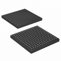
MCU CAP7 FPGA 225LFBGA
Manufacturer
Atmel
Series
CAP™r
Specifications of AT91CAP7E-NA-ZJ
Core Processor
ARM7
Core Size
16/32-Bit
Speed
80MHz
Connectivity
EBI/EMI, FPGA, IrDA, SPI, UART/USART, USB
Peripherals
DMA, POR, PWM, WDT
Number Of I /o
32
Program Memory Size
256KB (256K x 8)
Program Memory Type
ROM
Ram Size
160K x 8
Voltage - Supply (vcc/vdd)
1.08 V ~ 1.32 V
Data Converters
A/D 8x10b
Oscillator Type
Internal
Operating Temperature
-40°C ~ 85°C
Package / Case
225-LFBGA
Processor Series
AT91Mx
Core
ARM7TDMI
Data Bus Width
32 bit
3rd Party Development Tools
JTRACE-ARM-2M, MDK-ARM, RL-ARM, ULINK2
Lead Free Status / RoHS Status
Lead free / RoHS Compliant
Eeprom Size
-
Lead Free Status / Rohs Status
Details
Available stocks
Company
Part Number
Manufacturer
Quantity
Price


9.3
9.4
9.5
8549A–CAP–10/08
Reset Controller
Shut Down Controller
Clock Generator
• Based on two Power-on-Reset cells
• Status of the last reset
• Controls the internal resets and the NRST pin output
• Shut-Down and Wake-Up logic
• Embeds the Low Power, fast start-up 32kHz RC Oscillator
• Embeds the Low Power 32768Hz Slow Clock Oscillator
• Embeds the Main Oscillator
• Embeds PLLA primarily for generating processor and master clocks. For full-speed operation
• Embeds PLLB primarily for generating a 96 MHz clock that is divided down to generate the
on the ARM7TDMI processor, this PLL should be programmed to generate a 160 MHz clock
that must then be divided in half to generate the 80 MHz PCK and related clocks.
USB related clocks.
– one on VDDBU and one on VDDCORE
– Either general reset (VDDBU rising), wake-up reset (VDDCORE rising), software
– Allows shaping a reset signal for the external devices
– Software programmable assertion of the SHDN open-drain pin
– De-assertion Programmable on a WKUP pin level change or on alarm
– Provides the default Slow Clock SLCK to the system
– The SLCK is required for AT91CAP7E to start-up because it is the default clock for
– Requires an external 32768Hz crystal
– Optional Slow Clock SLCK source when a real-time timebase is required
– Requires an external crystal. For systems using the USB features, 12MHz is
– Oscillator bypass feature
– Supports 8 to 16MHz crystals. Recommend 12 MHz crystal if using the USB
– Generates input reference clock for the two PLLs.
– PLLA outputs an 80 to 240MHz clock
– Requires an external RC filter network
– PLLA has a 1MHz minimum input frequency
– Integrates an input divider to increase output accuracy
– PLLB uses an internal low-pass filter (LPF) and can output a 50 to 100 MHz clock
– PLLB and its internal low-pass filter (LPF) are tuned especially for generating a 96
– 12 MHz minimum input frequency
reset, user reset or watchdog reset
the ARM7TDMI at power-up.
recommended.
features of AT91CAP7E.
MHz clock with a 12 MHz input frequency
AT91CAP7E
25
Related parts for AT91CAP7E-NA-ZJ
Image
Part Number
Description
Manufacturer
Datasheet
Request
R

Part Number:
Description:
Customizable Microcontroller
Manufacturer:
ATMEL Corporation
Datasheet:

Part Number:
Description:
DEV KIT FOR AVR/AVR32
Manufacturer:
Atmel
Datasheet:
Part Number:
Description:
INTERVAL AND WIPE/WASH WIPER CONTROL IC WITH DELAY
Manufacturer:
ATMEL Corporation
Datasheet:
Part Number:
Description:
Low-Voltage Voice-Switched IC for Hands-Free Operation
Manufacturer:
ATMEL Corporation
Datasheet:
Part Number:
Description:
MONOLITHIC INTEGRATED FEATUREPHONE CIRCUIT
Manufacturer:
ATMEL Corporation
Datasheet:
Part Number:
Description:
AM-FM Receiver IC U4255BM-M
Manufacturer:
ATMEL Corporation
Datasheet:
Part Number:
Description:
Monolithic Integrated Feature Phone Circuit
Manufacturer:
ATMEL Corporation
Datasheet:
Part Number:
Description:
Multistandard Video-IF and Quasi Parallel Sound Processing
Manufacturer:
ATMEL Corporation
Datasheet:
Part Number:
Description:
High-performance EE PLD
Manufacturer:
ATMEL Corporation
Datasheet:
Part Number:
Description:
8-bit Flash Microcontroller
Manufacturer:
ATMEL Corporation
Datasheet:
Part Number:
Description:
2-Wire Serial EEPROM
Manufacturer:
ATMEL Corporation
Datasheet: