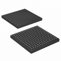
AT91CAP7E-NA-ZJ Atmel, AT91CAP7E-NA-ZJ Datasheet - Page 211

AT91CAP7E-NA-ZJ
Manufacturer Part Number
AT91CAP7E-NA-ZJ
Description
MCU CAP7 FPGA 225LFBGA
Manufacturer
Atmel
Series
CAP™r
Specifications of AT91CAP7E-NA-ZJ
Core Processor
ARM7
Core Size
16/32-Bit
Speed
80MHz
Connectivity
EBI/EMI, FPGA, IrDA, SPI, UART/USART, USB
Peripherals
DMA, POR, PWM, WDT
Number Of I /o
32
Program Memory Size
256KB (256K x 8)
Program Memory Type
ROM
Ram Size
160K x 8
Voltage - Supply (vcc/vdd)
1.08 V ~ 1.32 V
Data Converters
A/D 8x10b
Oscillator Type
Internal
Operating Temperature
-40°C ~ 85°C
Package / Case
225-LFBGA
Processor Series
AT91Mx
Core
ARM7TDMI
Data Bus Width
32 bit
3rd Party Development Tools
JTRACE-ARM-2M, MDK-ARM, RL-ARM, ULINK2
Lead Free Status / RoHS Status
Lead free / RoHS Compliant
Eeprom Size
-
Lead Free Status / Rohs Status
Details
Available stocks
Company
Part Number
Manufacturer
Quantity
Price
- Current page: 211 of 520
- Download datasheet (11Mb)
24.1.5.2
8549A–CAP–10/08
Divider and Phase Lock Loop Programming
The divider can be set between 1 and 255 in steps of 1. When a divider field (DIV) is set to 0, the
output of the corresponding divider and the PLL output is a continuous signal at level 0. On
reset, each DIV field is set to 0, thus the corresponding PLL input clock is set to 0.
The PLL allows multiplication of the divider’s outputs. The PLL clock signal has a frequency that
depends on the respective source signal frequency and on the parameters DIV and MUL. The
factor applied to the source signal frequency is (MUL + 1)/DIV. When MUL is written to 0, the
corresponding PLL is disabled and its power consumption is saved. Re-enabling the PLL can be
performed by writing a value higher than 0 in the MUL field.
Whenever the PLL is re-enabled or one of its parameters is changed, the LOCK bit (LOCKA or
LOCKB) in PMC_SR is automatically cleared. The values written in the PLLCOUNT field (PLLA-
COUNT or PLLBCOUNT) in CKGR_PLLR (CKGR_PLLAR or CKGR_PLLBR), are loaded in the
PLL counter. The PLL counter then decrements at the speed of the Slow Clock until it reaches 0.
At this time, the LOCK bit is set in PMC_SR and can trigger an interrupt to the processor. The
user has to load the number of Slow Clock cycles required to cover the PLL transient time into
the PLLCOUNT field. The transient time depends on the PLL filter. The initial state of the PLL
and its target frequency can be calculated using a specific tool provided by Atmel.
For PLLB, the values of DIV and MUL should be set to produce an input clock frequency of
12MHz and an output clock frequency of 96MHz for optimal operation for USB support. Any
other settings will likely result in result in reduced quality of the PLLB output clock.
AT91CAP7E
211
Related parts for AT91CAP7E-NA-ZJ
Image
Part Number
Description
Manufacturer
Datasheet
Request
R

Part Number:
Description:
Customizable Microcontroller
Manufacturer:
ATMEL Corporation
Datasheet:

Part Number:
Description:
DEV KIT FOR AVR/AVR32
Manufacturer:
Atmel
Datasheet:

Part Number:
Description:
INTERVAL AND WIPE/WASH WIPER CONTROL IC WITH DELAY
Manufacturer:
ATMEL Corporation
Datasheet:

Part Number:
Description:
Low-Voltage Voice-Switched IC for Hands-Free Operation
Manufacturer:
ATMEL Corporation
Datasheet:

Part Number:
Description:
MONOLITHIC INTEGRATED FEATUREPHONE CIRCUIT
Manufacturer:
ATMEL Corporation
Datasheet:

Part Number:
Description:
AM-FM Receiver IC U4255BM-M
Manufacturer:
ATMEL Corporation
Datasheet:

Part Number:
Description:
Monolithic Integrated Feature Phone Circuit
Manufacturer:
ATMEL Corporation
Datasheet:

Part Number:
Description:
Multistandard Video-IF and Quasi Parallel Sound Processing
Manufacturer:
ATMEL Corporation
Datasheet:

Part Number:
Description:
High-performance EE PLD
Manufacturer:
ATMEL Corporation
Datasheet:

Part Number:
Description:
8-bit Flash Microcontroller
Manufacturer:
ATMEL Corporation
Datasheet:

Part Number:
Description:
2-Wire Serial EEPROM
Manufacturer:
ATMEL Corporation
Datasheet:


