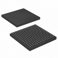
AT91CAP7E-NA-ZJ Atmel, AT91CAP7E-NA-ZJ Datasheet - Page 215

AT91CAP7E-NA-ZJ
Manufacturer Part Number
AT91CAP7E-NA-ZJ
Description
MCU CAP7 FPGA 225LFBGA
Manufacturer
Atmel
Series
CAP™r
Specifications of AT91CAP7E-NA-ZJ
Core Processor
ARM7
Core Size
16/32-Bit
Speed
80MHz
Connectivity
EBI/EMI, FPGA, IrDA, SPI, UART/USART, USB
Peripherals
DMA, POR, PWM, WDT
Number Of I /o
32
Program Memory Size
256KB (256K x 8)
Program Memory Type
ROM
Ram Size
160K x 8
Voltage - Supply (vcc/vdd)
1.08 V ~ 1.32 V
Data Converters
A/D 8x10b
Oscillator Type
Internal
Operating Temperature
-40°C ~ 85°C
Package / Case
225-LFBGA
Processor Series
AT91Mx
Core
ARM7TDMI
Data Bus Width
32 bit
3rd Party Development Tools
JTRACE-ARM-2M, MDK-ARM, RL-ARM, ULINK2
Lead Free Status / RoHS Status
Lead free / RoHS Compliant
Eeprom Size
-
Lead Free Status / Rohs Status
Details
Available stocks
Company
Part Number
Manufacturer
Quantity
Price
- Current page: 215 of 520
- Download datasheet (11Mb)
8549A–CAP–10/08
2. Checking the Main Oscillator Frequency (Optional):
3. Setting PLL A and divider A:
Once this register has been correctly configured, the user must wait for MOSCS field in the
PMC_SR register to be set. This can be done either by polling the status register or by wait-
ing the interrupt line to be raised if the associated interrupt to MOSCS has been enabled in
the PMC_IER register.
Code Example:
Start Up Time = 8 * OSCOUNT / SLCK = 56 Slow Clock Cycles.
So, the main oscillator will be enabled (MOSCS bit set) after 56 Slow Clock Cycles.
In some situations the user may need an accurate measure of the main oscillator frequency.
This measure can be accomplished via the CKGR_MCFR register.
Once the MAINRDY field is set in CKGR_MCFR register, the user may read the MAINF field
in CKGR_MCFR register. This provides the number of main clock cycles within sixteen slow
clock cycles.
All parameters necessary to configure PLL A and divider A are located in the CKGR_PLLAR
register.
It is important to note that Bit 29 must always be set to 1 when programming the
CKGR_PLLAR register.
The DIVA field is used to control the divider A itself. The user can program a value between
0 and 255. Divider A output is divider A input divided by DIVA. By default, DIVA parameter is
set to 0 which means that divider A is turned off.
The OUTA field is used to select the PLL A output frequency range.
The MULA field is the PLL A multiplier factor. This parameter can be programmed between
0 and 2047. If MULA is set to 0, PLL A will be turned off. Otherwise PLL A output frequency
is PLL A input frequency multiplied by (MULA + 1).
The PLLACOUNT field specifies the number of slow clock cycles before LOCKA bit is set in
the PMC_SR register after CKGR_PLLAR register has been written.
Once CKGR_PLLAR register has been written, the user is obliged to wait for the LOCKA bit
to be set in the PMC_SR register. This can be done either by polling the status register or by
waiting the interrupt line to be raised if the associated interrupt to LOCKA has been enabled
in the PMC_IER register.
All parameters in CKGR_PLLAR can be programmed in a single write operation. If at some
stage one of the following parameters, SRCA, MULA, DIVA is modified,
LOCKA bit will go low to indicate that PLL A is not ready yet. When PLL A is locked, LOCKA
will be set again. User has to wait for LOCKA bit to be set before using the PLL A output
clock.
Code Example:
write_register(CKGR_MOR,0x00000701)
write_register(CKGR_PLLAR,0x20030605)
AT91CAP7E
215
Related parts for AT91CAP7E-NA-ZJ
Image
Part Number
Description
Manufacturer
Datasheet
Request
R

Part Number:
Description:
Customizable Microcontroller
Manufacturer:
ATMEL Corporation
Datasheet:

Part Number:
Description:
DEV KIT FOR AVR/AVR32
Manufacturer:
Atmel
Datasheet:

Part Number:
Description:
INTERVAL AND WIPE/WASH WIPER CONTROL IC WITH DELAY
Manufacturer:
ATMEL Corporation
Datasheet:

Part Number:
Description:
Low-Voltage Voice-Switched IC for Hands-Free Operation
Manufacturer:
ATMEL Corporation
Datasheet:

Part Number:
Description:
MONOLITHIC INTEGRATED FEATUREPHONE CIRCUIT
Manufacturer:
ATMEL Corporation
Datasheet:

Part Number:
Description:
AM-FM Receiver IC U4255BM-M
Manufacturer:
ATMEL Corporation
Datasheet:

Part Number:
Description:
Monolithic Integrated Feature Phone Circuit
Manufacturer:
ATMEL Corporation
Datasheet:

Part Number:
Description:
Multistandard Video-IF and Quasi Parallel Sound Processing
Manufacturer:
ATMEL Corporation
Datasheet:

Part Number:
Description:
High-performance EE PLD
Manufacturer:
ATMEL Corporation
Datasheet:

Part Number:
Description:
8-bit Flash Microcontroller
Manufacturer:
ATMEL Corporation
Datasheet:

Part Number:
Description:
2-Wire Serial EEPROM
Manufacturer:
ATMEL Corporation
Datasheet:


