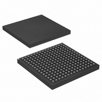
AT91CAP7E-NA-ZJ Atmel, AT91CAP7E-NA-ZJ Datasheet - Page 138

AT91CAP7E-NA-ZJ
Manufacturer Part Number
AT91CAP7E-NA-ZJ
Description
MCU CAP7 FPGA 225LFBGA
Manufacturer
Atmel
Series
CAP™r
Specifications of AT91CAP7E-NA-ZJ
Core Processor
ARM7
Core Size
16/32-Bit
Speed
80MHz
Connectivity
EBI/EMI, FPGA, IrDA, SPI, UART/USART, USB
Peripherals
DMA, POR, PWM, WDT
Number Of I /o
32
Program Memory Size
256KB (256K x 8)
Program Memory Type
ROM
Ram Size
160K x 8
Voltage - Supply (vcc/vdd)
1.08 V ~ 1.32 V
Data Converters
A/D 8x10b
Oscillator Type
Internal
Operating Temperature
-40°C ~ 85°C
Package / Case
225-LFBGA
Processor Series
AT91Mx
Core
ARM7TDMI
Data Bus Width
32 bit
3rd Party Development Tools
JTRACE-ARM-2M, MDK-ARM, RL-ARM, ULINK2
Lead Free Status / RoHS Status
Lead free / RoHS Compliant
Eeprom Size
-
Lead Free Status / Rohs Status
Details
Available stocks
Company
Part Number
Manufacturer
Quantity
Price
- Current page: 138 of 520
- Download datasheet (11Mb)
21.8.1
Figure 21-8. Standard Read Cycle
21.8.1.1
138
AT91CAP7E
Read Waveforms
NRD Waveform
NBS0,NBS1,
NBS2,NBS3,
A0, A1
D[31:0]
A[25:2]
MCK
NRD
NCS
The read cycle is shown on
The read cycle starts with the address setting on the memory address bus, i.e.:
The NRD signal is characterized by a setup timing, a pulse width and a hold timing.
1. NRD_SETUP: the NRD setup time is defined as the setup of address before the NRD
2. NRD_PULSE: the NRD pulse length is the time between NRD falling edge and NRD
3. NRD_HOLD: the NRD hold time is defined as the hold time of address after the NRD
NCS_RD_SETUP
falling edge;
rising edge;
rising edge.
{A[25:2], A1, A0} for 8-bit devices
{A[25:2], A1} for 16-bit devices
A[25:2] for 32-bit devices.
NRD_SETUP
Figure
NCS_RD_PULSE
NRD_CYCLE
NRD_PULSE
21-8.
NRD_HOLD
NCS_RD_HOLD
8549A–CAP–10/08
Related parts for AT91CAP7E-NA-ZJ
Image
Part Number
Description
Manufacturer
Datasheet
Request
R

Part Number:
Description:
Customizable Microcontroller
Manufacturer:
ATMEL Corporation
Datasheet:

Part Number:
Description:
DEV KIT FOR AVR/AVR32
Manufacturer:
Atmel
Datasheet:

Part Number:
Description:
INTERVAL AND WIPE/WASH WIPER CONTROL IC WITH DELAY
Manufacturer:
ATMEL Corporation
Datasheet:

Part Number:
Description:
Low-Voltage Voice-Switched IC for Hands-Free Operation
Manufacturer:
ATMEL Corporation
Datasheet:

Part Number:
Description:
MONOLITHIC INTEGRATED FEATUREPHONE CIRCUIT
Manufacturer:
ATMEL Corporation
Datasheet:

Part Number:
Description:
AM-FM Receiver IC U4255BM-M
Manufacturer:
ATMEL Corporation
Datasheet:

Part Number:
Description:
Monolithic Integrated Feature Phone Circuit
Manufacturer:
ATMEL Corporation
Datasheet:

Part Number:
Description:
Multistandard Video-IF and Quasi Parallel Sound Processing
Manufacturer:
ATMEL Corporation
Datasheet:

Part Number:
Description:
High-performance EE PLD
Manufacturer:
ATMEL Corporation
Datasheet:

Part Number:
Description:
8-bit Flash Microcontroller
Manufacturer:
ATMEL Corporation
Datasheet:

Part Number:
Description:
2-Wire Serial EEPROM
Manufacturer:
ATMEL Corporation
Datasheet:


