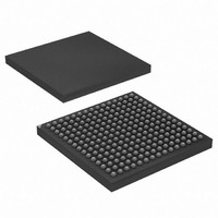
AT91CAP7E-NA-ZJ Atmel, AT91CAP7E-NA-ZJ Datasheet - Page 37

AT91CAP7E-NA-ZJ
Manufacturer Part Number
AT91CAP7E-NA-ZJ
Description
MCU CAP7 FPGA 225LFBGA
Manufacturer
Atmel
Series
CAP™r
Specifications of AT91CAP7E-NA-ZJ
Core Processor
ARM7
Core Size
16/32-Bit
Speed
80MHz
Connectivity
EBI/EMI, FPGA, IrDA, SPI, UART/USART, USB
Peripherals
DMA, POR, PWM, WDT
Number Of I /o
32
Program Memory Size
256KB (256K x 8)
Program Memory Type
ROM
Ram Size
160K x 8
Voltage - Supply (vcc/vdd)
1.08 V ~ 1.32 V
Data Converters
A/D 8x10b
Oscillator Type
Internal
Operating Temperature
-40°C ~ 85°C
Package / Case
225-LFBGA
Processor Series
AT91Mx
Core
ARM7TDMI
Data Bus Width
32 bit
3rd Party Development Tools
JTRACE-ARM-2M, MDK-ARM, RL-ARM, ULINK2
Lead Free Status / RoHS Status
Lead free / RoHS Compliant
Eeprom Size
-
Lead Free Status / Rohs Status
Details
Available stocks
Company
Part Number
Manufacturer
Quantity
Price
- Current page: 37 of 520
- Download datasheet (11Mb)
10.4.2
10.4.3
10.4.3.1
10.4.3.2
10.4.3.3
10.4.3.4
10.4.3.5
10.4.3.6
10.4.3.7
10.4.3.8
8549A–CAP–10/08
PIO Controller B Multiplexing
Resource Multiplexing
NAND Flash Interface
Compact Flash Interface
USARTs
Clock Outputs
Interrupt Lines
EBI
32-bit Data Bus
SPI
Table 10-2.
If not required, the NWAIT function (external wait request) can be deactivated by soft-ware
allowing this pin to be used as a PIO. Use of the NWAIT function prevents use of the Debug
Unit.
Using a 32-bit Data Bus prevents:
Using the NAND Flash interface prevents using the NCS3 and USART0.
Using the CompactFlash interface prevents using the USART0.
Using the SPI prevents use of NCS6, NCS7, and the ADC external trigger.
Using the USART0 prevents use of CompactFlash or NAND Flash.
Using the USART1 prevents using a full 32-bit bus for the EBI.
Using the clock outputs prevents use of either higher EBI address bits or a full 32-bit data bus
(see table 10-2).
Using FIQ prevents using the Debug Unit.
Using IRQ0 prevents the use of SPI_NPCS0.
Using IRQ1 prevents the use of SPI_NPCS1.
PIO Controller A
I/O Line
PA29
PA30
PA31
• The PIOB Port is part of the FPGA Interface, and its multiplexing is determined by that
• using the three Timer Counter channels’ outputs and trigger inputs
• using the USART1
• using two of the clock outputs (APMC_PCK2 and APMC_PCK3)
interface (see section
Multiplexing on PIO Controller A
Peripheral A
D29
D30
D31
11.4.2 ”PIO Controller B Multiplexing” on page
Peripheral B
TIMER2_TIOA2
TIMER1_TIOB1
TIMER2_TIOB2
Reset State
AT91CAP7E
47).
37
Related parts for AT91CAP7E-NA-ZJ
Image
Part Number
Description
Manufacturer
Datasheet
Request
R

Part Number:
Description:
Customizable Microcontroller
Manufacturer:
ATMEL Corporation
Datasheet:

Part Number:
Description:
DEV KIT FOR AVR/AVR32
Manufacturer:
Atmel
Datasheet:

Part Number:
Description:
INTERVAL AND WIPE/WASH WIPER CONTROL IC WITH DELAY
Manufacturer:
ATMEL Corporation
Datasheet:

Part Number:
Description:
Low-Voltage Voice-Switched IC for Hands-Free Operation
Manufacturer:
ATMEL Corporation
Datasheet:

Part Number:
Description:
MONOLITHIC INTEGRATED FEATUREPHONE CIRCUIT
Manufacturer:
ATMEL Corporation
Datasheet:

Part Number:
Description:
AM-FM Receiver IC U4255BM-M
Manufacturer:
ATMEL Corporation
Datasheet:

Part Number:
Description:
Monolithic Integrated Feature Phone Circuit
Manufacturer:
ATMEL Corporation
Datasheet:

Part Number:
Description:
Multistandard Video-IF and Quasi Parallel Sound Processing
Manufacturer:
ATMEL Corporation
Datasheet:

Part Number:
Description:
High-performance EE PLD
Manufacturer:
ATMEL Corporation
Datasheet:

Part Number:
Description:
8-bit Flash Microcontroller
Manufacturer:
ATMEL Corporation
Datasheet:

Part Number:
Description:
2-Wire Serial EEPROM
Manufacturer:
ATMEL Corporation
Datasheet:


