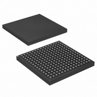
AT91CAP7E-NA-ZJ Atmel, AT91CAP7E-NA-ZJ Datasheet - Page 171

AT91CAP7E-NA-ZJ
Manufacturer Part Number
AT91CAP7E-NA-ZJ
Description
MCU CAP7 FPGA 225LFBGA
Manufacturer
Atmel
Series
CAP™r
Specifications of AT91CAP7E-NA-ZJ
Core Processor
ARM7
Core Size
16/32-Bit
Speed
80MHz
Connectivity
EBI/EMI, FPGA, IrDA, SPI, UART/USART, USB
Peripherals
DMA, POR, PWM, WDT
Number Of I /o
32
Program Memory Size
256KB (256K x 8)
Program Memory Type
ROM
Ram Size
160K x 8
Voltage - Supply (vcc/vdd)
1.08 V ~ 1.32 V
Data Converters
A/D 8x10b
Oscillator Type
Internal
Operating Temperature
-40°C ~ 85°C
Package / Case
225-LFBGA
Processor Series
AT91Mx
Core
ARM7TDMI
Data Bus Width
32 bit
3rd Party Development Tools
JTRACE-ARM-2M, MDK-ARM, RL-ARM, ULINK2
Lead Free Status / RoHS Status
Lead free / RoHS Compliant
Eeprom Size
-
Lead Free Status / Rohs Status
Details
Available stocks
Company
Part Number
Manufacturer
Quantity
Price
- Current page: 171 of 520
- Download datasheet (11Mb)
• BAT: Byte Access Type
This field is used only if DBW defines a 16- or 32-bit data bus.
• DBW: Data Bus Width
• TDF_CYCLES: Data Float Time
This field gives the integer number of clock cycles required by the external device to release the data after the rising edge
of the read controlling signal. The SMC always provide one full cycle of bus turnaround after the TDF_CYCLES period. The
external bus cannot be used by another chip select during TDF_CYCLES + 1 cycles. From 0 up to 15 TDF_CYCLES can
be set.
• TDF_MODE: TDF Optimization
1: TDF optimization is enabled.
0: TDF optimization is disabled.
• PMEN: Page Mode Enabled
1: Asynchronous burst read in page mode is applied on the corresponding chip select.
0: Standard read is applied.
• PS: Page Size
If page mode is enabled, this field indicates the size of the page in bytes.
8549A–CAP–10/08
• 1: Byte write access type:
• 0: Byte select access type:
– Write operation is controlled using NCS, NWR0, NWR1, NWR2, NWR3.
– Read operation is controlled using NCS and NRD.
– Write operation is controlled using NCS, NWE, NBS0, NBS1, NBS2 and NBS3
– Read operation is controlled using NCS, NRD, NBS0, NBS1, NBS2 and NBS3
– The number of TDF wait states is optimized using the setup period of the next read/write access.
– The number of TDF wait states is inserted before the next access begins.
0
0
1
1
0
0
1
1
DBW
PS
0
1
0
1
0
1
0
1
Data Bus Width
8-bit bus
16-bit bus
32-bit bus
Reserved
Page Size
4-byte page
8-byte page
16-byte page
32-byte page
AT91CAP7E
171
Related parts for AT91CAP7E-NA-ZJ
Image
Part Number
Description
Manufacturer
Datasheet
Request
R

Part Number:
Description:
Customizable Microcontroller
Manufacturer:
ATMEL Corporation
Datasheet:

Part Number:
Description:
DEV KIT FOR AVR/AVR32
Manufacturer:
Atmel
Datasheet:

Part Number:
Description:
INTERVAL AND WIPE/WASH WIPER CONTROL IC WITH DELAY
Manufacturer:
ATMEL Corporation
Datasheet:

Part Number:
Description:
Low-Voltage Voice-Switched IC for Hands-Free Operation
Manufacturer:
ATMEL Corporation
Datasheet:

Part Number:
Description:
MONOLITHIC INTEGRATED FEATUREPHONE CIRCUIT
Manufacturer:
ATMEL Corporation
Datasheet:

Part Number:
Description:
AM-FM Receiver IC U4255BM-M
Manufacturer:
ATMEL Corporation
Datasheet:

Part Number:
Description:
Monolithic Integrated Feature Phone Circuit
Manufacturer:
ATMEL Corporation
Datasheet:

Part Number:
Description:
Multistandard Video-IF and Quasi Parallel Sound Processing
Manufacturer:
ATMEL Corporation
Datasheet:

Part Number:
Description:
High-performance EE PLD
Manufacturer:
ATMEL Corporation
Datasheet:

Part Number:
Description:
8-bit Flash Microcontroller
Manufacturer:
ATMEL Corporation
Datasheet:

Part Number:
Description:
2-Wire Serial EEPROM
Manufacturer:
ATMEL Corporation
Datasheet:


