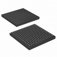
AT91CAP7E-NA-ZJ Atmel, AT91CAP7E-NA-ZJ Datasheet - Page 50

AT91CAP7E-NA-ZJ
Manufacturer Part Number
AT91CAP7E-NA-ZJ
Description
MCU CAP7 FPGA 225LFBGA
Manufacturer
Atmel
Series
CAP™r
Specifications of AT91CAP7E-NA-ZJ
Core Processor
ARM7
Core Size
16/32-Bit
Speed
80MHz
Connectivity
EBI/EMI, FPGA, IrDA, SPI, UART/USART, USB
Peripherals
DMA, POR, PWM, WDT
Number Of I /o
32
Program Memory Size
256KB (256K x 8)
Program Memory Type
ROM
Ram Size
160K x 8
Voltage - Supply (vcc/vdd)
1.08 V ~ 1.32 V
Data Converters
A/D 8x10b
Oscillator Type
Internal
Operating Temperature
-40°C ~ 85°C
Package / Case
225-LFBGA
Processor Series
AT91Mx
Core
ARM7TDMI
Data Bus Width
32 bit
3rd Party Development Tools
JTRACE-ARM-2M, MDK-ARM, RL-ARM, ULINK2
Lead Free Status / RoHS Status
Lead free / RoHS Compliant
Eeprom Size
-
Lead Free Status / Rohs Status
Details
Available stocks
Company
Part Number
Manufacturer
Quantity
Price
- Current page: 50 of 520
- Download datasheet (11Mb)
11.5.1
Figure 11-6. PIO interface to FPGA
11.5.2
50
AT91CAP7E
PIO-FPGA Connections
PIO-FPGA Access Routines
ARM Microcontroller
System
ARM
Since the processor must manage the flow of data to keep the PIO busy, there is a significant
overhead in processing time. Note that DMA is not possible using this architecture, therefore
the bandwidth is limited by the number of cycles the software programmer allocates for the
processor to communicate with the PIO. For example, if there is a routine running that de-
mands 100% of the processor cycles and concurrently there is serial data (e.g. SPI, USART,
USB, or TWI) to be transferred to/from the FPGA, one of these processes must wait. If the
data from the FPGA is not buffered on time, it will probably be overrun by the next byte/word.
To accomplish a proper data transfer to/from the FPGA, we need to transfer 32 bits of ad-
dress (or possibly less), 32 bits of data, and some control signals. For this approach, one will
need to use more that a 32 bit PIO port. At least 2 more PIO bits are necessary for control
signals.
The
Based on the resources shown above, we can define a software algorithm to transfer data
from/to FPGA.
Þ write_to_fpga: Algorithm to write 32 bits of data to FPGA, this assumes that, the
Þ read_from_fpga: Algorithm to read data from the FPGA, this assumes that, the direction
PIO 32
PIO 2
Data
Ctrl
bits
bits
direction of the bidirectional buffers in the PIO’s has been previously set.
of the bidirectional buffers in the PIO’s has been previously set.
Figure 11-6
PIO_DATA = ADDRESS; // Pass the address to write
PIO_CTRL = START | WR; // Send start of address cycle
PIO_CTRL = CLEAR; // Clear PIO ctrl, this ends the address cycle
PIO_DATA = DATA; // Set data to transfer
PIO_CTRL = START; // Data is ready in PIO
PIO_CTRL = CLEAR; // This end the data cycle
PIO_DATA = ADDRESS; // Set the address to read
PIO_CTRL = START | RD; // Send start of address cycle
PIO_CTRL = CLEAR; // Clear PIO ctrl, this ends the address cycle
shows the 32+2 PIO interface to a FPGA.
Address / Data
WR / RD _
Start
FPGA
Logic
FPGA
8549A–CAP–10/08
Related parts for AT91CAP7E-NA-ZJ
Image
Part Number
Description
Manufacturer
Datasheet
Request
R

Part Number:
Description:
Customizable Microcontroller
Manufacturer:
ATMEL Corporation
Datasheet:

Part Number:
Description:
DEV KIT FOR AVR/AVR32
Manufacturer:
Atmel
Datasheet:

Part Number:
Description:
INTERVAL AND WIPE/WASH WIPER CONTROL IC WITH DELAY
Manufacturer:
ATMEL Corporation
Datasheet:

Part Number:
Description:
Low-Voltage Voice-Switched IC for Hands-Free Operation
Manufacturer:
ATMEL Corporation
Datasheet:

Part Number:
Description:
MONOLITHIC INTEGRATED FEATUREPHONE CIRCUIT
Manufacturer:
ATMEL Corporation
Datasheet:

Part Number:
Description:
AM-FM Receiver IC U4255BM-M
Manufacturer:
ATMEL Corporation
Datasheet:

Part Number:
Description:
Monolithic Integrated Feature Phone Circuit
Manufacturer:
ATMEL Corporation
Datasheet:

Part Number:
Description:
Multistandard Video-IF and Quasi Parallel Sound Processing
Manufacturer:
ATMEL Corporation
Datasheet:

Part Number:
Description:
High-performance EE PLD
Manufacturer:
ATMEL Corporation
Datasheet:

Part Number:
Description:
8-bit Flash Microcontroller
Manufacturer:
ATMEL Corporation
Datasheet:

Part Number:
Description:
2-Wire Serial EEPROM
Manufacturer:
ATMEL Corporation
Datasheet:


