C8051F930-GQ Silicon Laboratories Inc, C8051F930-GQ Datasheet
C8051F930-GQ
Specifications of C8051F930-GQ
Available stocks


Related parts for C8051F930-GQ

C8051F930-GQ Summary of contents
Page 1
Supply Voltage 0 One-Cell Mode supports 0.9 to 1.8 V operation - Two-Cell Mode supports 1.8 to 3.6 V operation - Built-in dc-dc converter with 1.8 to 3.3 V output for use in one-cell mode - ...
Page 2
C8051F93x-C8051F92x 2 Rev. 1.1 ...
Page 3
Table of Contents 1. System Overview.................................................................................................... 18 1.1. CIP-51™ Microcontroller Core.......................................................................... 21 1.1.1. Fully 8051 Compatible.............................................................................. 21 1.1.2. Improved Throughput ............................................................................... 21 1.1.3. Additional Features .................................................................................. 21 1.2. Port Input/Output............................................................................................... 21 1.3. Serial Ports ....................................................................................................... 22 1.4. Programmable Counter Array ...
Page 4
C8051F93x-C8051F92x 7.2. Comparator Outputs ......................................................................................... 91 7.3. Comparator Response Time............................................................................. 92 7.4. Comparator Hysterisis ...................................................................................... 92 7.5. Comparator Register Descriptions.................................................................... 93 7.6. Comparator0 and Comparator1 Analog Multiplexers........................................ 97 8. CIP-51 Microcontroller ......................................................................................... 100 8.1. Instruction Set ................................................................................................. 101 8.1.1. Instruction ...
Page 5
Write Procedure ........................................................................... 146 13.2.Non-volatile Data Storage .............................................................................. 147 13.3.Security Options ............................................................................................. 147 13.4.Determining the Device Part Number at Run Time ........................................ 149 13.5.Flash Write and Erase Guidelines .................................................................. 150 13.5.1.VDD Maintenance and the VDD Monitor ............................................... 150 13.5.2.PSWE ...
Page 6
C8051F93x-C8051F92x 18.8.SmaRTClock (Real Time Clock) Reset .......................................................... 185 18.9.Software Reset ............................................................................................... 185 19. Clocking Sources ................................................................................................. 187 19.1.Programmable Precision Internal Oscillator ................................................... 188 19.2.Low Power Internal Oscillator......................................................................... 188 19.3.External Oscillator Drive Circuit...................................................................... 188 19.3.1.External Crystal Mode............................................................................ 188 19.3.2.External RC Mode.................................................................................. ...
Page 7
SMBus ................................................................................................................... 233 22.1.Supporting Documents ................................................................................... 234 22.2.SMBus Configuration...................................................................................... 234 22.3.SMBus Operation ........................................................................................... 235 22.3.1.Transmitter Vs. Receiver........................................................................ 235 22.3.2.Arbitration............................................................................................... 235 22.3.3.Clock Low Extension.............................................................................. 236 22.3.4.SCL Low Timeout................................................................................... 236 22.3.5.SCL High (SMBus Free) Timeout .......................................................... 236 22.4.Using the SMBus............................................................................................ 237 ...
Page 8
C8051F93x-C8051F92x 25.2.2.8-bit Timers with Auto-Reload................................................................ 289 25.2.3.Comparator 0/SmaRTClock Capture Mode ........................................... 290 25.3.Timer 3 .......................................................................................................... 294 25.3.1.16-bit Timer with Auto-Reload................................................................ 294 25.3.2.8-bit Timers with Auto-Reload................................................................ 295 25.3.3.Comparator 1/External Oscillator Capture Mode ................................... 296 26. Programmable Counter Array ............................................................................. 300 26.1.PCA ...
Page 9
... List of Figures 1. System Overview Figure 1.1. C8051F930 Block Diagram .................................................................... 19 Figure 1.2. C8051F931 Block Diagram .................................................................... 19 Figure 1.3. C8051F920 Block Diagram .................................................................... 20 Figure 1.4. C8051F921 Block Diagram .................................................................... 20 Figure 1.5. Port I/O Functional Block Diagram ......................................................... 22 Figure 1.6. PCA Block Diagram................................................................................ 23 Figure 1.7. ADC0 Functional Block Diagram............................................................ 24 Figure 1 ...
Page 10
C8051F93x-C8051F92x Figure 5.9. Temperature Sensor Error with 1-Point Calibration (V Figure 5.10. Voltage Reference Functional Block Diagram...................................... 86 6. Programmable Current Reference (IREF0) 7. Comparators Figure 7.1. Comparator 0 Functional Block Diagram ............................................... 90 Figure 7.2. Comparator 1 Functional Block ...
Page 11
Figure 21.2. Port I/O Cell Block Diagram ............................................................... 213 Figure 21.3. Crossbar Priority Decoder with No Pins Skipped ............................... 217 Figure 21.4. Crossbar Priority Decoder with Crystal Pins Skipped ........................ 218 22. SMBus Figure 22.1. SMBus Block Diagram ....................................................................... 233 ...
Page 12
C8051F93x-C8051F92x Figure 26.2. PCA Counter/Timer Block Diagram.................................................... 302 Figure 26.3. PCA Interrupt Block Diagram ............................................................. 302 Figure 26.4. PCA Capture Mode Diagram.............................................................. 304 Figure 26.5. PCA Software Timer Mode Diagram .................................................. 305 Figure 26.6. PCA High-Speed Output Mode Diagram............................................ 306 ...
Page 13
List of Tables 1. System Overview 2. Ordering Information Table 2.1. Product Selection Guide . . . . . . . . . . . . . . . . . . . . . . . . . . ...
Page 14
C8051F93x-C8051F92x 13. Flash Memory Table 13.1. Flash Security Summary . . . . . . . . . . . . . . . . . . . . . . . . . . . . . . . ...
Page 15
List of Registers SFR Definition 5.1. ADC0CN: ADC0 Control . . . . . . . . . . . . . . . . . . . . . . . . . . . . . . . ...
Page 16
C8051F93x-C8051F92x SFR Definition 14.1. PMU0CF: Power Management Unit Configuration SFR Definition 14.2. PCON: Power Management Control Register . . . . . . . . . . . . . . 163 SFR Definition 15.1. CRC0CN: CRC0 Control . . ...
Page 17
SFR Definition 21.20. P2MDIN: Port2 Input Mode . . . . . . . . . . . . . . . . . . . . . . . . . . . 231 SFR Definition 21.21. P2MDOUT: Port2 ...
Page 18
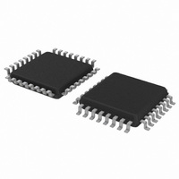
... Each device is specified for 0 1.8 to 3.6 V operation over the industrial temperature range (–40 to +85 °C). The Port I/O and RST pins are tolerant of input signals The C8051F930/20 are available in 32-pin QFN or LQFP packages and the C8051F931/21 are available in a 24-pin QFN package. ...
Page 19
... Oscillator GND External XTAL1 Oscillator XTAL2 Circuit XTAL3 SmaRTClock Oscillator XTAL4 System Clock Configuration Figure 1.1. C8051F930 Block Diagram CIP-51 8051 Power On Controller Core Reset/PMU 64 kB ISP Flash Wake Program Memory Reset 256 Byte SRAM Debug / C2CK/RST Programming 4096 Byte XRAM ...
Page 20
C8051F93x-C8051F92x CIP-51 8051 Power On Controller Core Reset/PMU 32 kB ISP Flash Wake Program Memory Reset 256 Byte SRAM Debug / C2CK/RST Programming 4096 Byte XRAM Hardware C2D Power Net VDD/DC+ VREG Analog Digital Power Power GND/DC- Precision 24.5 MHz ...
Page 21
... Port Input/Output Digital and analog resources are available through 24 I/O pins (C8051F930/20 I/O pins (C8051F931/21). Port pins are organized as three byte-wide ports. Port pins P0.0–P2.6 can be defined as digital or analog I/O. Digital I/O pins can be assigned to one of the internal digital resources or used as general purpose I/O (GPIO) ...
Page 22
C8051F93x-C8051F92x as GPIO and is shared with the C2 Interface Data signal (C2D). See Section “27. C2 Interface” on page 319 for more details. The designer has complete control over which digital and analog functions are assigned to individual Port ...
Page 23
Programmable Counter Array An on-chip Programmable Counter/Timer Array (PCA) is included in addition to the four 16-bit general pur- pose counter/timers. The PCA consists of a dedicated 16-bit counter/timer time base with six programma- ble capture/compare modules. The PCA ...
Page 24
C8051F93x-C8051F92x The ADC can sample the voltage at any of the GPIO pins (with the exception of P2.7) and has an on-chip attenuator that allows it to measure voltages up to twice the voltage reference. Additional ADC inputs include an ...
Page 25
P0.0 P2.6* Temp Sensor VBAT Digital Supply VDD/DC+ *P1.7-P2. 6 only available as inputs on 32- pin packages Figure 1.8. ADC0 Multiplexer Block Diagram 1.6. Programmable Current Reference (IREF0) C8051F93x-C8051F92x devices include an on-chip programmable current reference (source or sink) ...
Page 26
C8051F93x-C8051F92x CP0EN CP0OUT CP0RIF CP0FIF CP0HYP1 CP0HYP0 CP0HYN1 CP0HYN0 Analog Input Multiplexer Px.x CP0 + Px.x Px.x CP0 - Px.x Figure 1.9. Comparator 0 Functional Block Diagram CP1EN CP1OUT CP1RIF CP1FIF CP1HYP1 CP1HYP0 CP1HYN1 CP1HYN0 Analog Input Multiplexer Px.x CP1 ...
Page 27
... Ordering Information Table 2.1. Product Selection Guide C8051F930- 4352 C8051F930- 4352 C8051F931- 4352 C8051F920- 4352 C8051F920- 4352 C8051F921- 4352 C8051F93x-C8051F92x ...
Page 28
C8051F93x-C8051F92x 3. Pinout and Package Definitions Table 3.1. Pin Definitions for the C8051F92x-C8051F93x Pin Numbers Name ‘F920/30 ‘F921/31 VBAT DC+ DC– GND GND 2 2 DCEN 4 4 RST/ 6 ...
Page 29
Table 3.1. Pin Definitions for the C8051F92x-C8051F93x (Continued) Pin Numbers Name ‘F920/30 ‘F921/31 P0 REF P0 AGND P0 XTAL1 P0 XTAL2 P0 P0 P0.6 26 ...
Page 30
C8051F93x-C8051F92x Table 3.1. Pin Definitions for the C8051F92x-C8051F93x (Continued) Pin Numbers Name ‘F920/30 ‘F921/31 P1 AD0* P1 AD1* P1 AD2* P1 AD3* P1 AD4* P1 AD5* P1.6 18 ...
Page 31
Table 3.1. Pin Definitions for the C8051F92x-C8051F93x (Continued) Pin Numbers Name ‘F920/30 ‘F921/31 P2.1* 15 AD9* P2.2* 14 AD10* P2.3* 13 AD11* P2.4* 12 ALE* P2.5* 11 RD* P2.6* 8 WR* *Note: Available only on the C8051F920/30. C8051F93x-C8051F92x Type Description ...
Page 32
... C8051F93x-C8051F92x GND/DC- 1 GND 2 VDD/DC+ 3 C8051F930/20-GM DCEN 4 VBAT 5 RST/C2CK 6 P2.7/C2D 7 P2.6/WR 8 Figure 3.1. QFN-32 Pinout Diagram (Top View) 32 Top View Rev. 1.1 24 P1.0/AD0 23 P1.1/AD1 22 P1.2/AD2 21 P1.3/AD3 20 P1.4/AD4 19 P1.5/AD5 18 P1.6/AD6 17 P1.7/AD7 ...
Page 33
GND/DC- 1 GND 2 VDD/DC+ 3 C8051F931/21-GM DCEN 4 VBAT 5 RST/C2CK 6 Figure 3.2. QFN-24 Pinout Diagram (Top View) C8051F93x-C8051F92x Top View Rev. 1.1 18 P0.6/CNVSTR 17 P0.7/IREF0 16 P1.0 15 P1.1 14 P1.2 13 P1.3 33 ...
Page 34
... C8051F93x-C8051F92x 1 GND / DC- 2 GND 3 VDD / DC+ C8051F930/20-GQ 4 DCEN 5 VBAT 6 RST / C2CK P2.7 / C2D 7 P2 Figure 3.3. LQFP-32 Pinout Diagram (Top View) 34 Top View Rev. 1.1 24 P1.0 / AD0 23 P1.1 / AD1 22 P1.2 / AD2 21 P1.3 / AD3 20 P1.4 / AD4 19 P1.5 / AD5 18 P1.6 / AD6 17 P1.7 / AD7 ...
Page 35
Figure 3.4. QFN-32 Package Drawing Table 3.2. QFN-32 Package Dimensions Dimension Min Typ Max A 0.80 0.9 1.00 A1 0.00 0.02 0.05 b 0.18 0.25 0.30 D 5.00 BSC D2 3.20 3.30 3.40 e 0.50 BSC E 5.00 BSC Notes: ...
Page 36
C8051F93x-C8051F92x Figure 3.5. Typical QFN-32 Landing Diagram 36 Rev. 1.1 ...
Page 37
Table 3.3. PCB Land Pattern Dimension Notes: General 1. All dimensions shown are in millimeters (mm) unless otherwise noted. 2. This Land Pattern Design is based on the IPC-7351 guidelines. Solder Mask Design ...
Page 38
C8051F93x-C8051F92x Figure 3.6. QFN-24 Package Drawing Table 3.4. QFN-24 Package Dimensions Dimension Min Typ A 0.70 0.75 A1 0.00 0.02 b 0.18 0.25 D 4.00 BSC D2 2.55 2.70 e 0.50 BSC E 4.00 BSC E2 2.55 2.70 Notes: 1. ...
Page 39
C8051F93x-C8051F92x Figure 3.7. Typical QFN-24 Landing Diagram Rev. 1.1 39 ...
Page 40
C8051F93x-C8051F92x Table 3.5. PCB Land Pattern Dimension Notes: General 1. All dimensions shown are in millimeters (mm) unless otherwise noted. 2. This Land Pattern Design is based on the IPC-7351 guidelines. Solder Mask ...
Page 41
Figure 3.8. LQFP-32 Package Diagram Table 3.6. LQFP-32 Package Dimensions Dimension Min Typ A — — A1 0.05 — A2 1.35 1.40 b 0.30 0.37 c 0.09 — D 9.00 BSC. D1 7.00 BSC e 0.80 BSC Notes: 1. All ...
Page 42
C8051F93x-C8051F92x Figure 3.9. Typical LQFP-32 Landing Diagram Table 3.7. PCB Land Pattern Dimension Notes: General 1. All dimensions shown are in millimeters (mm) unless otherwise noted. 2. This Land Pattern Design is based on the ...
Page 43
Electrical Characteristics Throughout the Electrical Characteristics chapter, “VDD” refers to the VDD/DC+ Supply Voltage. 4.1. Absolute Maximum Specifications Table 4.1. Absolute Maximum Ratings Parameter Ambient temperature under bias Storage Temperature Voltage on any Port I/O Pin or RST with ...
Page 44
C8051F93x-C8051F92x 4.2. Electrical Characteristics Table 4.2. Global Electrical Characteristics –40 to +85 °C, 25 MHz system clock unless otherwise specified. See "AN358: Optimizing Low Power Operation of the ‘F9xx" for details on how to achieve the supply current specifications listed ...
Page 45
Table 4.2. Global Electrical Characteristics (Continued) –40 to +85 °C, 25 MHz system clock unless otherwise specified. See "AN358: Optimizing Low Power Operation of the ‘F9xx" for details on how to achieve the supply current specifications listed in this table. ...
Page 46
C8051F93x-C8051F92x 4200 F < 10 MHz 4100 4000 Oneshot Enabled 3900 3800 3700 3600 3500 3400 3300 3200 3100 3000 2900 2800 2700 2600 2500 2400 2300 2200 2100 2000 1900 1800 1700 1600 1500 1400 1300 1200 1100 1000 ...
Page 47
4200 4100 4000 3900 3800 3700 3600 3500 3400 3300 3200 3100 3000 2900 2800 2700 2600 2500 2400 2300 2200 2100 2000 1900 1800 1700 1600 1500 1400 1300 1200 1100 1000 900 800 700 600 500 400 300 ...
Page 48
C8051F93x-C8051F92x SWSEL = 1 91.0 90.0 89.0 88.0 87.0 86.0 85.0 84.0 83.0 82.0 81.0 80.0 79.0 78.0 77.0 76.0 75.0 74.0 73.0 72.0 71.0 70.0 0.68 uH Inductor, 1210 package, ESR = 0.1 Ohms 69.0 VDD/DC+ = 2V, Minimum ...
Page 49
SWSEL = 1 85.0 84.0 83.0 82.0 81.0 80.0 79.0 78.0 77.0 76.0 75.0 74.0 73.0 72.0 71.0 70.0 69.0 68.0 67.0 0.68 uH Inductor, 1210 package, ESR = 0.1 Ohms 66.0 VDD/DC+ = 3V, Minimum Pulse Width = 0ns ...
Page 50
C8051F93x-C8051F92x 85.0 80.0 75.0 70.0 65.0 60.0 55.0 50.0 0.68 uH Inductor, 1210 package, ESR = 0.1 Ohms SWSEL = 1, VDD/DC+ = 2V, Minimum Pulse Width = 40ns 45.0 40.0 35.0 0.00 0.25 0.50 0.75 Figure 4.5. Typical DC-DC ...
Page 51
Inductor, 1210 package, ESR = 0.1 Ohms 1000 SWSEL = 1, VDD/DC+ = 1.9V, Load Current = 80 uA 950 900 850 800 750 700 650 600 550 500 450 400 350 300 250 200 0.9 1.0 ...
Page 52
C8051F93x-C8051F92x Table 4.3. Port I/O DC Electrical Characteristics V = 1.8 to 3.6 V, –40 to +85 °C unless otherwise specified. DD Parameters Output High Voltage High Drive Strength, PnDRV IOH = –3 mA, Port I/O push-pull IOH ...
Page 53
C8051F93x-C8051F92x Typical VOH (High Drive Mode) 3.6 3.3 3 2.7 2.4 2.1 1.8 1.5 1.2 0 Load Current (mA) Typical VOH (Low Drive Mode) 3.6 3.3 3 2.7 2.4 2.1 1.8 1.5 1.2 ...
Page 54
C8051F93x-C8051F92x 1.8 1.7 1.6 1.5 1.4 1.3 1.2 1.1 1 0.9 0.8 0.7 0.6 0 1.8 1.7 1.6 1.5 1.4 1.3 1.2 1.1 1 0.9 0.8 0.7 0.6 0.5 0 Figure 4.8. Typical VOH Curves, 0.9–1.8 V ...
Page 55
C8051F93x-C8051F92x Typical VOL (High Drive Mode) 1.8 1.5 1.2 0.9 0.6 0.3 0 -80 -70 -60 -50 -40 -30 Load Current (mA) Typical VOL (Low Drive Mode) 1.8 1.5 1.2 0.9 0.6 0 ...
Page 56
C8051F93x-C8051F92x 0.5 0.4 0.3 0.2 0 0.5 0.4 0.3 VDD = 1.8V 0.2 VDD = 1.5V VDD = 1.2V 0.1 VDD = 0. Figure 4.10. Typical VOL Curves, 0.9–1 Typical VOL (High Drive ...
Page 57
Table 4.4. Reset Electrical Characteristics V = 1.8 to 3.6 V, –40 to +85 °C unless otherwise specified. DD Parameter RST Output Low Voltage I = 1.4 mA, OL RST Input High Voltage V = 2 ...
Page 58
... One-cell mode Table 4.6. Flash Electrical Characteristics V = 1.8 to 3.6 V, –40 to +85 °C unless otherwise specified. DD Parameter Flash Size C8051F930/1 C8051F920/1 Scratchpad Size Endurance Erase Cycle Time Write Cycle Time *Note: 1024 bytes at addresses 0xFC00 to 0xFFFF are reserved. Table 4.7. Internal Precision Oscillator Electrical Characteristics V = 1.8 to 3.6 V ...
Page 59
Table 4.9. ADC0 Electrical Characteristics V = 1.8 to 3.6V V, VREF = 1.65 V (REFSL[1:0] = 11), DD Parameter Resolution Integral Nonlinearity Differential Nonlinearity Guaranteed Monotonic Offset Error Full Scale Error Dynamic performance (10 kHz sine-wave single-ended input, 1 ...
Page 60
C8051F93x-C8051F92x Table 4.10. Temperature Sensor Electrical Characteristics V – = 1 +85 °C unless otherwise specified. DD Parameter Linearity Slope Slope Error* Offset Temp = 25 °C Offset Error* Temp = 25 °C Temperature Sensor ...
Page 61
Table 4.12. IREF0 Electrical Characteristics V – = 1 +85 °C, unless otherwise specified. DD Parameter Resolution High Current Mode, Source Output Compliance Range Integral Nonlinearity Differential Nonlinearity Offset Error High Current Mode, Source Full ...
Page 62
C8051F93x-C8051F92x Table 4.13. Comparator Electrical Characteristics V = 1.8 to 3.6 V, –40 to +85 °C unless otherwise noted. DD Parameter Response Time: * Mode 2 1 Response Time: * Mode ...
Page 63
Table 4.13. Comparator Electrical Characteristics V = 1.8 to 3.6 V, –40 to +85 °C unless otherwise noted. DD Parameter Hysteresis Mode 0 Hysteresis 1 Hysteresis 2 Hysteresis 3 Hysteresis 4 Mode 1 Hysteresis 1 Hysteresis 2 Hysteresis 3 Hysteresis ...
Page 64
C8051F93x-C8051F92x Table 4.14. DC-DC Converter (DC0) Electrical Characteristics –40 to +85 °C unless otherwise specified. VBAT = 0.9 to 1.8 V, Parameter Input Voltage Range Input Inductor Value Input Inductor Current Rating Inductor DC Resistance Input Capacitor Value Source Impedance ...
Page 65
SAR ADC with 16-bit Auto-Averaging Accumulator and Autonomous Low Power Burst Mode The ADC0 on the C8051F93x-C8051F92x is a 300 ksps, 10-bit successive-approximation-register (SAR) ADC with integrated track-and-hold and programmable window detector. ADC0 also has an autonomous low ...
Page 66
C8051F93x-C8051F92x 5.1. Output Code Formatting The registers ADC0H and ADC0L contain the high and low bytes of the output conversion code from the ADC at the completion of each conversion. Data can be right-justified or left-justified, depending on the setting ...
Page 67
Modes of Operation ADC0 has a maximum conversion speed of 300 ksps. The ADC0 conversion clock (SARCLK divided version of the system clock when Burst Mode is disabled (BURSTEN = 0 divided version of the ...
Page 68
C8051F93x-C8051F92x 5.2.2. Tracking Modes Each ADC0 conversion must be preceded by a minimum tracking time in order for the converted result to be accurate. The minimum tracking time is given in Table 4.9. The AD0TM bit in register ADC0CN controls ...
Page 69
Burst Mode Burst Mode is a power saving feature that allows ADC0 to remain in a low power state between conver- sions. When Burst Mode is enabled, ADC0 wakes from a low power state, accumulates 16, ...
Page 70
C8051F93x-C8051F92x 5.2.4. Settling Time Requirements A minimum amount of tracking time is required before each conversion can be performed, to allow the sampling capacitor voltage to settle. This tracking time is determined by the AMUX0 resistance, the ADC0 sampling capacitance, ...
Page 71
Gain Setting The ADC has gain settings of 1x and 0.5x mode, the full scale reading of the ADC is determined directly 0.5x mode, the full-scale reading of the ADC occurs when the ...
Page 72
C8051F93x-C8051F92x SFR Definition 5.1. ADC0CN: ADC0 Control Bit 7 6 Name AD0EN BURSTEN AD0INT R/W R/W Type Reset 0 0 SFR Page = 0x0; SFR Address = 0xE8; bit-addressable; Bit Name 7 AD0EN ADC0 Enable. 0: ADC0 Disabled (low-power shutdown). ...
Page 73
SFR Definition 5.2. ADC0CF: ADC0 Configuration Bit 7 6 Name AD0SC[4:0] Type Reset 1 1 SFR Page = 0x0; SFR Address = 0xBC Bit Name 7:3 AD0SC[4:0] ADC0 SAR Conversion Clock Divider. SAR Conversion clock is derived from FCLK by ...
Page 74
C8051F93x-C8051F92x SFR Definition 5.3. ADC0AC: ADC0 Accumulator Configuration Bit 7 6 Name Reserved AD0AE R/W W Type Reset 0 0 SFR Page = 0x0; SFR Address = 0xBA Bit Name 7 Reserved Reserved. Read = 0b. 6 AD0AE ADC0 Accumulate ...
Page 75
SFR Definition 5.4. ADC0PWR: ADC0 Burst Mode Power-Up Time Bit 7 6 Name Reserved Type Reset SFR Page = 0xF; SFR Address = 0xBA Bit Name 7 Reserved Reserved. Read = 0b; Must write 0b. 6:4 ...
Page 76
C8051F93x-C8051F92x SFR Definition 5.5. ADC0TK: ADC0 Burst Mode Track Time Bit 7 6 Name Type Reset SFR Page = 0xF; SFR Address = 0xBD Bit Name 7:6 Unused Unused. Read = 00b; Write = Don’t Care. ...
Page 77
SFR Definition 5.6. ADC0H: ADC0 Data Word High Byte Bit 7 6 Name Type 0 0 Reset SFR Page = 0x0; SFR Address = 0xBE Bit Name Description 7:0 ADC0[15:8] ADC0 Data Word High Byte. Note: If Accumulator shifting is ...
Page 78
C8051F93x-C8051F92x 5.4. Programmable Window Detector The ADC Programmable Window Detector continuously compares the ADC0 output registers to user- programmed limits, and notifies the system when a desired condition is detected. This is especially effective in an interrupt-driven system, saving code ...
Page 79
SFR Definition 5.10. ADC0LTH: ADC0 Less-Than High Byte Bit 7 6 Name Type 0 0 Reset SFR Page = 0x0; SFR Address = 0xC6 Bit Name 7:0 AD0LT[15:8] ADC0 Less-Than High Byte. Most Significant Byte of the 16-bit Less-Than window ...
Page 80
C8051F93x-C8051F92x 5.4.1. Window Detector In Single-Ended Mode Figure 5.5 shows two example ADC0LTH:ADC0LTL = 0x0080 (128d) and ADC0GTH:ADC0GTL = 0x0040 (64d). The input voltage can range from 0 to VREF x (1023/1024) with respect to GND, and is represented by ...
Page 81
ADC0 Analog Multiplexer ADC0 on C8051F93x-C8051F92x has an analog multiplexer, referred to as AMUX0. AMUX0 selects the positive inputs to the single-ended ADC0. Any of the following may be selected as the positive input: Port I/O pins, the on-chip ...
Page 82
C8051F93x-C8051F92x SFR Definition 5.12. ADC0MX: ADC0 Input Channel Select Bit 7 6 Name R R Type 0 0 Reset SFR Page = 0x0; SFR Address = 0xBB Bit Name 7:5 Unused Unused. Read = 000b; Write = Don’t Care. 4:0 ...
Page 83
Temperature Sensor An on-chip temperature sensor is included on the C8051F93x-C8051F92x which can be directly accessed via the ADC multiplexer in single-ended configuration. To use the ADC to measure the temperature sensor, the ADC mux channel should select the ...
Page 84
C8051F93x-C8051F92x 5.6.1. Calibration The uncalibrated temperature sensor output is extremely linear and suitable for relative temperature mea- surements (see Table 4.10 for linearity specifications). For absolute temperature measurements, offset and/or gain calibration is recommended. Typically a 1-point (offset) calibration includes ...
Page 85
SFR Definition 5.13. TOFFH: ADC0 Data Word High Byte Bit 7 6 Name R R Type Varies Varies Varies Reset SFR Page = 0xF; SFR Address = 0x86 Bit Name 7:0 TOFF[9:2] Temperature Sensor Offset High Bits. Most Significant Bits ...
Page 86
C8051F93x-C8051F92x 5.7. Voltage and Ground Reference Options The voltage reference MUX is configurable to use an externally connected voltage reference, one of two internal voltage references, or one of two power supply voltages (see Figure 5.10). The ground reference MUX ...
Page 87
External Voltage References To use an external voltage reference, REFSL[1:0] should be set to 00 and the internal 1.68 V precision ref- erence should be disabled by setting REFOE to 0. Bypass capacitors should be added as recommended by ...
Page 88
C8051F93x-C8051F92x SFR Definition 5.15. REF0CN: Voltage Reference Control Bit 7 6 Name REFGND R R Type 0 0 Reset SFR Page = 0x0; SFR Address = 0xD1 Bit Name 7:6 Unused Unused. Read = 00b; Write = Don’t Care. 5 ...
Page 89
Programmable Current Reference (IREF0) C8051F93x-C8051F92x devices include an on-chip programmable current reference (source or sink) with two output current settings: Low Power Mode and High Current Mode. The maximum current output in Low Power Mode is 63 µA (1 ...
Page 90
C8051F93x-C8051F92x 7. Comparators C8051F93x-C8051F92x devices include two on-chip programmable voltage comparators: Comparator 0 (CPT0) is shown in Figure 7.1; Comparator 1 (CPT1) is shown in Figure 7.2. The two comparators operate identically, but may differ in their ability to be ...
Page 91
Comparator Outputs When a comparator is enabled, its output is a logic 1 if the voltage at the positive input is higher than the voltage at the negative input. When disabled, the comparator output is a logic 0. The ...
Page 92
C8051F93x-C8051F92x 7.3. Comparator Response Time Comparator response time may be configured in software via the CPTnMD registers described on “CPT0MD: Comparator 0 Mode Selection” on page 94 and “CPT1MD: Comparator 1 Mode Selection” on page 96. Four response time settings ...
Page 93
Comparator Register Descriptions The SFRs used to enable and configure the comparators are described in the following register descriptions. A Comparator must be enabled by setting the CPnEN bit to logic 1 before it can be used. From an ...
Page 94
C8051F93x-C8051F92x SFR Definition 7.2. CPT0MD: Comparator 0 Mode Selection Bit 7 6 Name CP0RIE Type R/W R Reset 1 0 SFR Page = All Pages; SFR Address = 0x9D Bit Name 7 Reserved Reserved. Read = 1b, Must Write 1b. ...
Page 95
SFR Definition 7.3. CPT1CN: Comparator 1 Control Bit 7 6 Name CP1EN CP1OUT CP1RIF Type R/W R Reset 0 0 SFR Page= 0x0; SFR Address = 0x9A Bit Name 7 CP1EN Comparator1 Enable Bit. 0: Comparator1 Disabled. 1: Comparator1 Enabled. ...
Page 96
C8051F93x-C8051F92x SFR Definition 7.4. CPT1MD: Comparator 1 Mode Selection Bit 7 6 Name CP1RIE Type R/W R Reset 1 0 SFR Page = 0x0; SFR Address = 0x9C Bit Name 7 Reserved Reserved. Read = 1b, Must Write 1b. 6 ...
Page 97
Comparator0 and Comparator1 Analog Multiplexers Comparator0 and Comparator1 on C8051F93x-C8051F92x devices have analog input multiplexers to con- nect Port I/O pins and internal signals the comparator inputs; CP0+/CP0- are the positive and negative input multiplexers for Comparator0 and CP1+/CP1- ...
Page 98
C8051F93x-C8051F92x SFR Definition 7.5. CPT0MX: Comparator0 Input Channel Select Bit 7 6 Name CMX0N[3:0] R/W R/W Type 1 1 Reset SFR Page = 0x0; SFR Address = 0x9F Bit Name 7:4 CMX0N Comparator0 Negative Input Selection. Selects the negative input ...
Page 99
SFR Definition 7.6. CPT1MX: Comparator1 Input Channel Select Bit 7 6 Name CMX1N[3:0] R/W R/W Type 1 1 Reset SFR Page = 0x0; SFR Address = 0x9E Bit Name 7:4 CMX1N Comparator1 Negative Input Selection. Selects the negative input channel ...
Page 100
C8051F93x-C8051F92x 8. CIP-51 Microcontroller The MCU system controller core is the CIP-51 microcontroller. The CIP-51 is fully compatible with the MCS-51™ instruction set; standard 803x/805x assemblers and compilers can be used to develop soft- ware. The MCU family has a ...
Page 101
With the CIP-51's maximum system clock at 25 MHz, it has a peak throughput of 25 MIPS. The CIP-51 has a total of 109 instructions. The table below shows the total number of instructions that require each execu- tion time. ...
Page 102
C8051F93x-C8051F92x Table 8.1. CIP-51 Instruction Set Summary Mnemonic ADD A, Rn Add register to A ADD A, direct Add direct byte to A ADD A, @Ri Add indirect RAM to A ADD A, #data Add immediate to A ADDC A, ...
Page 103
Table 8.1. CIP-51 Instruction Set Summary (Continued) Mnemonic CLR A Clear A CPL A Complement Rotate A left RLC A Rotate A left through Carry RR A Rotate A right RRC A Rotate A right through Carry ...
Page 104
C8051F93x-C8051F92x Table 8.1. CIP-51 Instruction Set Summary (Continued) Mnemonic ANL C, /bit AND complement of direct bit to Carry ORL C, bit OR direct bit to carry ORL C, /bit OR complement of direct bit to Carry MOV C, bit ...
Page 105
Notes on Registers, Operands and Addressing Modes: Rn—Register R0–R7 of the currently selected register bank. @Ri—Data RAM location addressed indirectly through R0 or R1. rel—8-bit, signed (twos complement) offset relative to the first byte of the following instruction. Used by ...
Page 106
C8051F93x-C8051F92x 8.2. CIP-51 Register Descriptions Following are descriptions of SFRs related to the operation of the CIP-51 System Controller. Reserved bits should not be set to logic l. Future product versions may use these bits to implement new features in ...
Page 107
SFR Definition 8.3. SP: Stack Pointer Bit 7 6 Name Type Reset 0 0 SFR Page = All Pages; SFR Address = 0x81 Bit Name 7:0 SP[7:0] Stack Pointer. The Stack Pointer holds the location of the top of the ...
Page 108
C8051F93x-C8051F92x SFR Definition 8.6. PSW: Program Status Word Bit 7 6 Name CY AC Type R/W R/W Reset 0 0 SFR Page = All Pages; SFR Address = 0xD0; Bit-Addressable Bit Name 7 CY Carry Flag. This bit is set ...
Page 109
... Program and data memory share the same address space but are accessed via different instruction types. The memory organization of the C8051F93x-C8051F92x device family is shown in Figure 9 RAM / (FLA SH) C8051F930/1 0x03FF Scrachpad M em ory (D ATA only) 0x0000 ...
Page 110
... The CIP-51 core has program memory space. The C8051F93x-C8051F92x implements 64 kB (C8051F930/ (C8051F920/1) of this program memory space as in-system, re-programmable Flash memory, organized in a contiguous block from addresses 0x0000 to 0xFBFF (C8051F930/1) or 0x7FFF (C8051F920/1). The address 0xFBFF (C8051F930/1) or 0x7FFF (C8051F920/1) serves as the security lock byte for the device. Any addresses above the lock byte are reserved. ...
Page 111
Data Memory The C8051F93x-C8051F92x device family includes 4352 bytes of RAM data memory. 256 bytes of this memory is mapped into the internal RAM space of the 8051. 4096 bytes of this memory is on-chip “exter- nal” memory. The ...
Page 112
C8051F93x-C8051F92x 9.2.1.3. Stack A programmer's stack can be located anywhere in the 256-byte data memory. The stack area is desig- nated using the Stack Pointer (SP) SFR. The SP will point to the last location used. The next value pushed ...
Page 113
... External Data Memory Interface and On-Chip XRAM The C8051F92x-C8051F93x MCUs include on-chip RAM mapped into the external data memory space (XRAM). 32-pin devices (C8051F930 and C8051F920) also have an External Data Memory Interface which can be used to access off-chip memories and memory-mapped devices connected to the GPIO ports ...
Page 114
C8051F93x-C8051F92x 10.2. Configuring the External Memory Interface for Off-Chip Access Configuring the External Memory Interface for off-chip memory space access consists of four steps: 1. Configure the Output Modes of the associated port pins as either push-pull or open-drain (push-pull ...
Page 115
Multiplexed External Memory Interface For a Multiplexed external memory interface, the Data Bus and the lower 8-bits of the Address Bus share the same Port pins: AD[7:0]. For most devices with an 8-bit interface, the upper address bits are ...
Page 116
C8051F93x-C8051F92x A[11:8] ALE E AD[7:0] ADDRESS/DATA BUS Figure 10.2. Multiplexed to Non-Multiplexed Configuration Example 116 ADDRESS BUS A[11:8] 74HC373 A[7: (Optional) 8 I/O[7: Rev. 1 ...
Page 117
External Memory Interface Operating Modes The external data memory space can be configured in one of four operating modes, shown in Figure 10.3, based on the EMIF Mode bits in the EMI0CF register (SFR Definition 10.2). These modes are ...
Page 118
C8051F93x-C8051F92x 10.5.3. Split Mode with Bank Select When EMI0CF.[3:2] are set to 10, the XRAM memory map is split into two areas, on-chip space and off- chip space. • Effective addresses below the on-chip XRAM boundary will access on-chip XRAM ...
Page 119
EMIF Special Function Registers The special function registers used by the EMIF are EMI0CN, EMI0CF, and EMI0TC. These registers are described in the following register descriptions. SFR Definition 10.1. EMI0CN: External Memory Interface Control Bit 7 6 Name R/W ...
Page 120
C8051F93x-C8051F92x SFR Definition 10.2. EMI0CF: External Memory Configuration Bit 7 6 Name R/W R/W Type 0 0 Reset SFR Page = 0x0; SFR Address = 0xAB Bit Name 7:4 Unused Unused. Read = 0000b. Write = Don’t Care. 3:2 EMD ...
Page 121
SFR Definition 10.3. EMI0TC: External Memory Timing Control Bit 7 6 Name EAS[1:0] R/W R/W Type 1 1 Reset SFR Page = 0x0; SFR Address = 0xAF Bit Name 7:4 EAS Address Setup Time Select Bits. Controls the timing parameter ...
Page 122
C8051F93x-C8051F92x 10.8. EMIF Timing Diagrams 10.8.1. Multiplexed 16-bit MOVX: EMI0CF[3:2] = 01, 10 ADDR[11:8] EMIF ADDRESS (8 LSBs) from AD[7:0] DPL T ALEH ALE /WR /RD ADDR[11:8] EMIF ADDRESS (8 LSBs) from AD[7:0] DPL T ALEH ALE /RD ...
Page 123
Multiplexed 8-bit MOVX without Bank Select: EMI0CF[3: 11. ADDR[11:8] EMIF ADDRESS (8 LSBs) from AD[7: ALEH ALE /WR /RD ADDR[11:8] EMIF ADDRESS (8 LSBs) from AD[7: ...
Page 124
C8051F93x-C8051F92x 10.8.2.1.Multiplexed 8-bit MOVX with Bank Select: EMI0CF[3:2] = 10. ADDR[11:8] EMIF ADDRESS (4 MSBs) from EMI0CN EMIF ADDRESS (8 LSBs) from AD[7: ALEH ALE /WR /RD ADDR[11:8] EMIF ADDRESS (4 MSBs) from EMI0CN EMIF ...
Page 125
Table 10.1. AC Parameters for External Memory Interface Parameter Description T Address/Control Setup Time ACS T Address/Control Pulse Width ACW T Address/Control Hold Time ACH T Address Latch Enable High Time ALEH T Address Latch Enable Low Time ALEL T ...
Page 126
C8051F93x-C8051F92x 11. Special Function Registers The direct-access data memory locations from 0x80 to 0xFF constitute the special function registers (SFRs). The SFRs provide control and data exchange with the C8051F93x-C8051F92x's resources and peripherals. The CIP-51 controller core duplicates the SFRs ...
Page 127
SFR Paging To accommodate more than 128 SFRs in the 0x80 to 0xFF address space, SFR paging has been implemented. By default, all SFR accesses target SFR Page 0x0 to allow access to the registers listed in Table 11.1. ...
Page 128
C8051F93x-C8051F92x SFR Definition 11.1. SFR Page: SFR Page Bit 7 6 Name Type Reset 0 0 SFR Page = All Pages; SFR Address = 0xA7 Bit Name 7:0 SFRPAGE[7:0] SFR Page. Specifies the SFR Page used when reading, writing, or ...
Page 129
Table 11.3. Special Function Registers (Continued) SFRs are listed in alphabetical order. All undefined SFR locations are reserved Register Address SFR Page CPT1MD 0x9C 0x0 CPT1MX 0x9E 0x0 CRC0AUTO 0x96 0xF CRC0CN 0x92 0xF CRC0CNT 0x97 0xF CRC0DAT 0x91 0xF ...
Page 130
C8051F93x-C8051F92x Table 11.3. Special Function Registers (Continued) SFRs are listed in alphabetical order. All undefined SFR locations are reserved Register Address SFR Page P0SKIP 0xD4 0x0 P1 0x90 All P1DRV 0xA5 0xF P1MASK 0xBF 0x0 P1MAT 0xCF 0x0 P1MDIN 0xF2 ...
Page 131
Table 11.3. Special Function Registers (Continued) SFRs are listed in alphabetical order. All undefined SFR locations are reserved Register Address SFR Page PCA0MD 0xD9 0x0 PCA0PWM 0xDF 0x0 PCON 0x87 0x0 PMU0CF 0xB5 0x0 PSCTL 0x8F 0x0 PSW 0xD0 All ...
Page 132
C8051F93x-C8051F92x Table 11.3. Special Function Registers (Continued) SFRs are listed in alphabetical order. All undefined SFR locations are reserved Register Address SFR Page TMOD 0x89 0x0 TMR2CN 0xC8 0x0 TMR2H 0xCD 0x0 TMR2L 0xCC 0x0 TMR2RLH 0xCB 0x0 TMR2RLL 0xCA ...
Page 133
Interrupt Handler The C8051F93x-C8051F92x microcontroller family includes an extended interrupt system supporting mul- tiple interrupt sources and two priority levels. The allocation of interrupt sources between on-chip peripher- als and external input pins varies according to the specific version ...
Page 134
C8051F93x-C8051F92x 12.3. Interrupt Priorities Each interrupt source can be individually programmed to one of two priority levels: low or high. A low prior- ity interrupt service routine can be preempted by a high priority interrupt. A high priority interrupt cannot ...
Page 135
Table 12.1. Interrupt Summary Interrupt Interrupt Source Vector 0x0000 Reset 0x0003 External Interrupt 0 (INT0) Timer 0 Overflow 0x000B 0x0013 External Interrupt 1 (INT1) Timer 1 Overflow 0x001B UART0 0x0023 Timer 2 Overflow 0x002B SPI0 0x0033 SMB0 0x003B SmaRTClock Alarm ...
Page 136
C8051F93x-C8051F92x 12.5. Interrupt Register Descriptions The SFRs used to enable the interrupt sources and set their priority level are described in the following register descriptions. Refer to the data sheet section associated with a particular on-chip peripheral for information regarding ...
Page 137
SFR Definition 12.1. IE: Interrupt Enable Bit 7 6 Name EA ESPI0 Type R/W R/W Reset 0 0 SFR Page = All Pages; SFR Address = 0xA8; Bit-Addressable Bit Name 7 EA Enable All Interrupts. Globally enables/disables all interrupts. It ...
Page 138
C8051F93x-C8051F92x SFR Definition 12.2. IP: Interrupt Priority Bit 7 6 PSPI0 Name Type R R/W Reset 1 0 SFR Page = 0x0; SFR Address = 0xB8; Bit-Addressable Bit Name 7 Unused Unused. Read = 1b, Write = don't care. 6 ...
Page 139
SFR Definition 12.3. EIE1: Extended Interrupt Enable 1 Bit 7 6 Name ET3 ECP1 Type R/W R/W Reset 0 0 SFR Page = All Pages; SFR Address = 0xE6 Bit Name 7 ET3 Enable Timer 3 Interrupt. This bit sets ...
Page 140
C8051F93x-C8051F92x SFR Definition 12.4. EIP1: Extended Interrupt Priority 1 Bit 7 6 Name PT3 PCP1 Type R/W R/W Reset 0 0 SFR Page = All Pages; SFR Address = 0xF6 Bit Name 7 PT3 Timer 3 Interrupt Priority Control. This ...
Page 141
SFR Definition 12.5. EIE2: Extended Interrupt Enable 2 Bit 7 6 Name R/W R/W Type Reset 0 0 SFR Page = All Pages;SFR Address = 0xE7 Bit Name 7:4 Unused Unused. Read = 0000b. Write = Don’t care. 3 ESPI1 ...
Page 142
C8051F93x-C8051F92x SFR Definition 12.6. EIP2: Extended Interrupt Priority 2 Bit 7 6 Name R R Type Reset 0 0 SFR Page = All Pages; SFR Address = 0xF7 Bit Name 7:4 Unused Unused. Read = 0000b. Write = Don’t care. ...
Page 143
External Interrupts INT0 and INT1 The INT0 and INT1 external interrupt sources are configurable as active high or low, edge or level sensi- tive. The IN0PL (INT0 Polarity) and IN1PL (INT1 Polarity) bits in the IT01CF register select active ...
Page 144
C8051F93x-C8051F92x SFR Definition 12.7. IT01CF: INT0/INT1 Configuration Bit 7 6 Name IN1PL IN1SL[2:0] Type R/W Reset 0 0 SFR Page = 0x0; SFR Address = 0xE4 Bit Name 7 IN1PL INT1 Polarity. 0: INT1 input is active low. 1: INT1 ...
Page 145
Flash Memory On-chip, re-programmable Flash memory is included for program code and non-volatile data storage. The Flash memory can be programmed in-system through the C2 interface or by software using the MOVX write instruction. Once cleared to logic 0, ...
Page 146
C8051F93x-C8051F92x 13.1.2. Flash Erase Procedure The Flash memory is organized in 1024-byte pages. The erase operation applies to an entire page (setting all bytes in the page to 0xFF). To erase an entire 1024-byte page, perform the following steps: 1. ...
Page 147
... Flash Security Lock Byte is unlocked when no other Flash pages are locked (all bits of the Lock Byte are 1) and locked when any other Flash pages are locked (any bit of the Lock Byte is 0). See the C8051F930 example below. Security Lock Byte: ...
Page 148
C8051F93x-C8051F92x The level of Flash security depends on the Flash access method. The three Flash access methods that can be restricted are reads, writes, and erases from the C2 debug interface, user firmware executing on unlocked pages, and user firmware ...
Page 149
... The part number can be determined by reading the value of the Flash byte at address 0xFFFE. The value of the Flash byte at address 0xFFFE can be decoded as follows: 0x56—C8051F930 0x5E—C8051F931 0xB1—C8051F920 0xB3—C8051F921 C8051F93x-C8051F92x Rev ...
Page 150
C8051F93x-C8051F92x 13.5. Flash Write and Erase Guidelines Any system which contains routines which write or erase Flash memory from software involves some risk that the write or erase routines will execute unintentionally if the CPU is operating outside its specified ...
Page 151
PSWE Maintenance 7. Reduce the number of places in code where the PSWE bit (b0 in PSCTL) is set There should be exactly one routine in code that sets PSWE write Flash ...
Page 152
C8051F93x-C8051F92x 13.6. Minimizing Flash Read Current The Flash memory in the C8051F93x-C8051F92x devices is responsible for a substantial portion of the total digital supply current when the device is executing code. Below are suggestions to minimize Flash read current. 1. ...
Page 153
SFR Definition 13.1. PSCTL: Program Store R/W Control Bit 7 6 Name Type R R Reset 0 0 SFR Page =0x0; SFR Address = 0x8F Bit Name 7:3 Unused Unused. Read = 00000b, Write = don’t care. 2 SFLE Scratchpad ...
Page 154
C8051F93x-C8051F92x SFR Definition 13.2. FLKEY: Flash Lock and Key Bit 7 6 Name Type Reset 0 0 SFR Page = 0x0; SFR Address = 0xB6 Bit Name 7:0 FLKEY[7:0] Flash Lock and Key Register. Write: This register provides a lock ...
Page 155
SFR Definition 13.3. FLSCL: Flash Scale Bit 7 6 Name BYPASS Type R R/W Reset 0 0 SFR Page = 0x0; SFR Address = 0xB6 Bit Name 7 Reserved Reserved. Always Write BYPASS Flash Read Timing One-Shot ...
Page 156
C8051F93x-C8051F92x 14. Power Management C8051F93x-C8051F92x devices support 5 power modes: Normal, Idle, Stop, Suspend, and Sleep. The power management unit (PMU0) allows the device to enter and wake-up from the available power modes. A brief description of each power mode ...
Page 157
Normal Mode The MCU is fully functional in Normal Mode. Figure 14.1 shows the on-chip power distribution to various peripherals. There are three supply voltages powering various sections of the chip: VBAT, VDD/DC+, and the 1.8 V internal core ...
Page 158
... Stop Mode is a legacy 8051 power mode; it will not result in optimal power savings. Sleep or Suspend mode will provide more power savings if the MCU needs to be inactive for a long period of time. On C8051F930, C8051F931, C8051F920, and C8051F921 devices, the Precision Oscillator Bias is not automatically disabled and should be disabled by software to achieve the lowest possible Stop mode cur- rent ...
Page 159
Suspend Mode Setting the Suspend Mode Select bit (PMU0CF.6) causes the system clock to be gated off and all internal oscillators disabled. All digital logic (timers, communication peripherals, interrupts, CPU, etc.) stops functioning until one of the enabled wake-up ...
Page 160
C8051F93x-C8051F92x GPIO pins configured as digital inputs can be used during sleep mode as wakeup sources using the port match feature. In two-cell mode, they will maintain the same input level specs in sleep mode as they have in normal ...
Page 161
Determining the Event that Caused the Last Wakeup When waking from idle mode, the CPU will vector to the interrupt which caused it to wake up. When waking from stop mode, the RSTSRC register may be read to determine ...
Page 162
C8051F93x-C8051F92x SFR Definition 14.1. PMU0CF: Power Management Unit Configuration Bit 7 6 Name SLEEP SUSPEND CLEAR W W Type 0 0 Reset SFR Page = 0x0; SFR Address = 0xB5 Bit Name Description 7 SLEEP Sleep Mode Select 6 SUSPEND ...
Page 163
SFR Definition 14.2. PCON: Power Management Control Register Bit 7 6 Name Type 0 0 Reset SFR Page = All Pages; SFR Address = 0x87 Bit Name Description 7:2 GF[5:0] General Purpose Flags 1 STOP Stop Mode Select 0 IDLE ...
Page 164
C8051F93x-C8051F92x 15. Cyclic Redundancy Check Unit (CRC0) C8051F93x-C8051F92x devices include a cyclic redundancy check unit (CRC0) that can perform a CRC using a 16-bit or 32-bit polynomial. CRC0 accepts a stream of 8-bit data written to the CRC0IN register. CRC0 ...
Page 165
The 16-bit C8051F93x-C8051F92x CRC algorithm can be described by the following code: unsigned short UpdateCRC (unsigned short CRC_acc, unsigned char CRC_input) { unsigned char i; #define POLY 0x1021 // Create the CRC "dividend" for polynomial arithmetic (binary arithmetic // with ...
Page 166
C8051F93x-C8051F92x 15.2. Preparing for a CRC Calculation To prepare CRC0 for a CRC calculation, software should select the desired polynomial and set the initial value of the result. Two polynomials are available: 0x1021 (16-bit) and 0x04C11DB7 (32-bit). The CRC0 result ...
Page 167
SFR Definition 15.1. CRC0CN: CRC0 Control Bit 7 6 Name R/W R/W Type 0 0 Reset SFR Page = 0xF; SFR Address = 0x92 Bit Name 7:5 Unused Unused. Read = 000b; Write = Don’t Care. 4 CRC0SEL CRC0 Polynomial ...
Page 168
C8051F93x-C8051F92x SFR Definition 15.2. CRC0IN: CRC0 Data Input Bit 7 6 Name Type Reset 0 0 SFR Page = 0xF; SFR Address = 0x93 Bit Name 7:0 CRC0IN[7:0] CRC0 Data Input. Each write to CRC0IN results in the written data ...
Page 169
SFR Definition 15.4. CRC0AUTO: CRC0 Automatic Control Bit 7 6 Name AUTOEN CRCDONE Type Reset 0 1 SFR Page = 0xF; SFR Address = 0x96 Bit Name 7 AUTOEN Automatic CRC Calculation Enable. When AUTOEN is set to 1, any ...
Page 170
C8051F93x-C8051F92x 15.5. CRC0 Bit Reverse Feature CRC0 includes hardware to reverse the bit order of each bit in a byte as shown in Figure 15.2. Each byte of data written to CRC0FLIP is read back bit reversed. For example, if ...
Page 171
On-Chip DC-DC Converter (DC0) C8051F93x-C8051F92x devices include an on-chip dc-dc converter to allow operation from a single cell battery with a supply voltage as low as 0.9 V. The dc-dc converter is a switching boost converter with an input ...
Page 172
C8051F93x-C8051F92x 16.1. Startup Behavior On initial power-on, the dc-dc converter outputs a constant 50% duty cycle until there is sufficient voltage on the output capacitor to maintain regulation. The size of the output capacitor and the amount of load cur- ...
Page 173
High Power Applications The dc-dc converter is designed to provide the system with output power, however, it can safely provide up to 100 mW of output power without any risk of damage to the device. For ...
Page 174
C8051F93x-C8051F92x 16.4. Enabling the DC-DC Converter On power-on reset, the state of the DCEN pin is sampled to determine if the device will power up in one- cell or two-cell mode. In two-cell mode, the dc-dc converter always remains disabled. ...
Page 175
Minimizing Power Supply Noise To minimize noise on the power supply lines, the GND and GND/DC- pins should be kept separate, as shown in Figure 16.2; one or the other should be connected to the pc board ground plane. ...
Page 176
C8051F93x-C8051F92x outputs during sleep mode, then the VDD/DC+ output can be made to float during Sleep mode by setting the VDDSLP bit in the DC0CF register to 1. Setting this bit can provide power savings in two ways. First, if ...
Page 177
DC-DC Converter Register Descriptions The SFRs used to configure the dc-dc converter are described in the following register descriptions. The reset values for these registers can be used as-is in most systems; therefore, no software intervention or initialization is ...
Page 178
C8051F93x-C8051F92x SFR Definition 16.2. DC0CF: DC-DC Converter Configuration Bit 7 6 Name Reserved CLKDIV[1:0] Type R R/W Reset 0 0 SFR Page = 0x0; SFR Address = 0x96 Bit Name 7 Reserved Reserved. Read = 0b; Must write 0b. 6:5 ...
Page 179
Voltage Regulator (VREG0) C8051F93x-C8051F92x devices include an internal voltage regulator (VREG0) to regulate the internal core supply to 1.8 V from a VDD/DC+ supply of 1.8 to 3.6 V. Electrical characteristics for the on-chip regulator are specified in the ...
Page 180
C8051F93x-C8051F92x 18. Reset Sources Reset circuitry allows the controller to be easily placed in a predefined default condition. On entry to this reset state, the following occur: • CIP-51 halts program execution • Special Function Registers (SFRs) are initialized to ...
Page 181
Power-On (VBAT Supply Monitor) Reset During power-up, the device is held in a reset state and the RST pin is driven low until additional delay occurs before the device is released from reset; the delay ...
Page 182
C8051F93x-C8051F92x 18.2. Power-Fail (VDD/DC+ Supply Monitor) Reset C8051F93x-C8051F92x devices have a VDD/DC+ Supply Monitor that is enabled and selected as a reset source after each power-on or power-fail reset. When enabled and selected as a reset source, any power down ...
Page 183
Important Notes: • The Power-on Reset (POR) delay is not incurred after a VDD/DC+ supply monitor reset. See Section “4. Electrical Characteristics” on page 43 for complete electrical characteristics of the VDD/DC+ moni- tor. • Software should take care not ...
Page 184
C8051F93x-C8051F92x 18.3. External Reset The external RST pin provides a means for external circuitry to force the device into a reset state. Assert- ing an active-low signal on the RST pin generates a reset; an external pullup and/or decoupling of ...
Page 185
Flash Error Reset If a Flash read/write/erase or program read targets an illegal address, a system reset is generated. This may occur due to any of the following: • A Flash write or erase is attempted above user code ...
Page 186
C8051F93x-C8051F92x SFR Definition 18.2. RSTSRC: Reset Source Bit 7 6 Name RTC0RE FERROR C0RSEF R/W R Type Varies Varies Varies Reset SFR Page = 0x0; SFR Address = 0xEF. Bit Name Description 7 RTC0RE SmaRTClock Reset Enable and Flag 6 ...
Page 187
Clocking Sources C8051F93x-C8051F92x devices include a programmable precision internal oscillator, an external oscillator drive circuit, a low power internal oscillator, and a SmaRTClock real time clock oscillator. The precision internal oscillator can be enabled/disabled and calibrated using the OSCICN ...
Page 188
C8051F93x-C8051F92x 19.1. Programmable Precision Internal Oscillator All C8051F93x-C8051F92x devices include a programmable precision internal oscillator that may be selected as the system clock. OSCICL is factory calibrated to obtain a 24.5 MHz frequency. See Section “4. Electrical Characteristics” on page ...
Page 189
MHz 15 pF Figure 19.2. 25 MHz External Crystal Example Important Note on External Crystals: Crystal oscillator circuits are quite sensitive to PCB layout. The crystal should be placed as close as possible to the XTAL pins ...
Page 190
C8051F93x-C8051F92x 19.3.2. External RC Mode network is used as the external oscillator, the circuit should be configured as shown in Figure 19.1, Option 2. The RC network should be added to XTAL2, and XTAL2 should be configured ...
Page 191
When the RC oscillator is first enabled, the external oscillator valid detector allows software to determine when oscillation has stabilized. The recommended procedure for starting the RC oscillator is: 1. Configure XTAL2 for analog I/O and disable the digital output ...
Page 192
C8051F93x-C8051F92x 19.3.4. External CMOS Clock Mode If an external CMOS clock is used as the external oscillator, the clock should be directly routed into XTAL2. The XTAL2 pin should be configured as a digital input. XTAL1 is not used in ...
Page 193
Special Function Registers for Selecting and Configuring the System Clock The clocking sources on C8051F93x-C8051F92x devices are enabled and configured using the OSCICN, OSCICL, OSCXCN and the SmaRTClock internal registers. See Section “20. SmaRTClock (Real Time Clock)” on page ...
Page 194
C8051F93x-C8051F92x SFR Definition 19.2. OSCICN: Internal Oscillator Control Bit 7 6 Name IOSCEN IFRDY R/W R Type 0 0 Reset SFR Page = 0x0; SFR Address = 0xB2 Bit Name 7 IOSCEN Internal Oscillator Enable. 0: Internal oscillator disabled. 1: ...
Page 195
SFR Definition 19.4. OSCXCN: External Oscillator Control Bit 7 6 Name XCLKVLD XOSCMD[2: Type 0 0 Reset SFR Page = 0x0; SFR Address = 0xB1 Bit Name 7 XCLKVLD External Oscillator Valid Flag. Provides External Oscillator status and ...
Page 196
C8051F93x-C8051F92x 20. SmaRTClock (Real Time Clock) C8051F93x-C8051F92x devices include an ultra low power 32-bit SmaRTClock Peripheral (Real Time Clock) with alarm. The SmaRTClock has a dedicated 32 kHz oscillator that can be configured for use with or without a crystal. ...
Page 197
SmaRTClock Interface The SmaRTClock Interface consists of three registers: RTC0KEY, RTC0ADR, and RTC0DAT. These inter- face registers are located on the CIP-51’s SFR map and provide access to the SmaRTClock internal regis- ters listed in Table 20.1. The SmaRTClock ...
Page 198
C8051F93x-C8051F92x 20.1.2. Using RTC0ADR and RTC0DAT to Access SmaRTClock Internal Registers The SmaRTClock internal registers can be read and written using RTC0ADR and RTC0DAT. The RTC0ADR register selects the SmaRTClock internal register that will be targeted by subsequent reads or ...
Page 199
SmaRTClock Interface Autoread Feature When Autoread is enabled, each read from RTC0DAT initiates the next indirect read operation on the SmaRTClock internal register selected by RTC0ADR. Software should set the BUSY bit once at the beginning of each series ...
Page 200
C8051F93x-C8051F92x SFR Definition 20.1. RTC0KEY: SmaRTClock Lock and Key Bit 7 6 Name Type 0 0 Reset SFR Page = 0x0; SFR Address = 0xAE Bit Name 7:0 RTC0ST SmaRTClock Interface Lock/Key and Status. Locks/unlocks the SmaRTClock interface when written. ...