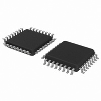
C8051F930-GQ Silicon Laboratories Inc, C8051F930-GQ Datasheet - Page 250

C8051F930-GQ
Manufacturer Part Number
C8051F930-GQ
Description
IC 8051 MCU 64K FLASH 32-LQFP
Manufacturer
Silicon Laboratories Inc
Series
C8051F9xxr
Specifications of C8051F930-GQ
Program Memory Type
FLASH
Program Memory Size
64KB (64K x 8)
Package / Case
32-LQFP
Core Processor
8051
Core Size
8-Bit
Speed
25MHz
Connectivity
SMBus (2-Wire/I²C), SPI, UART/USART
Peripherals
Brown-out Detect/Reset, POR, PWM, Temp Sensor, WDT
Number Of I /o
24
Ram Size
4.25K x 8
Voltage - Supply (vcc/vdd)
0.9 V ~ 3.6 V
Data Converters
A/D 23x10b
Oscillator Type
Internal
Operating Temperature
-40°C ~ 85°C
Processor Series
C8051F9x
Core
8051
Data Bus Width
8 bit
Data Ram Size
4.25 KB
Interface Type
I2C/SMBus/SPI/UART
Maximum Clock Frequency
25 MHz
Number Of Programmable I/os
24
Number Of Timers
4
Operating Supply Voltage
0.9 V to 3.6 V
Maximum Operating Temperature
+ 85 C
Mounting Style
SMD/SMT
3rd Party Development Tools
PK51, CA51, A51, ULINK2
Development Tools By Supplier
C8051F930DK
Minimum Operating Temperature
- 40 C
On-chip Adc
23-ch x 10-bit
No. Of I/o's
24
Ram Memory Size
4KB
Cpu Speed
25MHz
No. Of Timers
4
Rohs Compliant
Yes
Lead Free Status / RoHS Status
Lead free / RoHS Compliant
For Use With
336-1478 - PLATFORM PROG TOOLSTCK F920,F930336-1477 - PLATFORM PROG TOOLSTCK F920,F930336-1473 - KIT DEV C8051F920,F921,F930,F931336-1472 - BOARD TARGET/PROTO W/C8051F930
Eeprom Size
-
Lead Free Status / Rohs Status
Lead free / RoHS Compliant
Other names
336-1466
Available stocks
Company
Part Number
Manufacturer
Quantity
Price
Company:
Part Number:
C8051F930-GQ
Manufacturer:
SILICON
Quantity:
3 500
Company:
Part Number:
C8051F930-GQ
Manufacturer:
Silicon Laboratories Inc
Quantity:
10 000
Company:
Part Number:
C8051F930-GQR
Manufacturer:
Silicon Laboratories Inc
Quantity:
10 000
Part Number:
C8051F930-GQR
Manufacturer:
SILICON LABS/èٹ¯ç§‘
Quantity:
20 000
C8051F93x-C8051F92x
22.5.4. Read Sequence (Slave)
During a read sequence, an SMBus master reads data from a slave device. The slave in this transfer will
be a receiver during the address byte, and a transmitter during all data bytes. When slave events are
enabled (INH = 0), the interface enters Slave Receiver Mode (to receive the slave address) when a START
followed by a slave address and direction bit (READ in this case) is received. If hardware ACK generation
is disabled, upon entering Slave Receiver Mode, an interrupt is generated and the ACKRQ bit is set. The
software must respond to the received slave address with an ACK, or ignore the received slave address
with a NACK. If hardware ACK generation is enabled, the hardware will apply the ACK for a slave address
which matches the criteria set up by SMB0ADR and SMB0ADM. The interrupt will occur after the ACK
cycle.
If the received slave address is ignored (by software or hardware), slave interrupts will be inhibited until the
next START is detected. If the received slave address is acknowledged, zero or more data bytes are
transmitted. If the received slave address is acknowledged, data should be written to SMB0DAT to be
transmitted. The interface enters Slave Transmitter Mode, and transmits one or more bytes of data. After
each byte is transmitted, the master sends an acknowledge bit; if the acknowledge bit is an ACK,
SMB0DAT should be written with the next data byte. If the acknowledge bit is a NACK, SMB0DAT should
not be written to before SI is cleared (an error condition may be generated if SMB0DAT is written following
a received NACK while in Slave Transmitter Mode). The interface exits Slave Transmitter Mode after
receiving a STOP. Note that the interface will switch to Slave Receiver Mode if SMB0DAT is not written
following a Slave Transmitter interrupt. Figure 22.8 shows a typical slave read sequence. Two transmitted
data bytes are shown, though any number of bytes may be transmitted. All of the “data byte transferred”
interrupts occur after the ACK cycle in this mode, regardless of whether hardware ACK generation is
enabled.
22.6. SMBus Status Decoding
The current SMBus status can be easily decoded using the SMB0CN register. The appropriate actions to
take in response to an SMBus event depend on whether hardware slave address recognition and ACK
generation is enabled or disabled. Table 22.5 describes the typical actions when hardware slave address
recognition and ACK generation is disabled. Table 22.6 describes the typical actions when hardware slave
address recognition and ACK generation is enabled. In the tables, STATUS VECTOR refers to the four
upper bits of SMB0CN: MASTER, TXMODE, STA, and STO. The shown response options are only the
typical responses; application-specific procedures are allowed as long as they conform to the SMBus
specification. Highlighted responses are allowed by hardware but do not conform to the SMBus
specification.
250
S
Received by SMBus
Interface
Transmitted by
SMBus Interface
SLA
Figure 22.8. Typical Slave Read Sequence
R
A
Interrupts with Hardware ACK Disabled (EHACK = 0)
Interrupts with Hardware ACK Enabled (EHACK = 1)
Data Byte
Rev. 1.1
A
S = START
P = STOP
N = NACK
R = READ
SLA = Slave Address
Data Byte
N
P


