DF38602RFT10 Renesas Electronics America, DF38602RFT10 Datasheet - Page 24
DF38602RFT10
Manufacturer Part Number
DF38602RFT10
Description
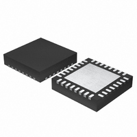
MCU 3V 16K 32-QFN
Manufacturer
Renesas Electronics America
Series
H8® H8/300H SLPr
Datasheet
1.DF38602RFT10.pdf
(554 pages)
Specifications of DF38602RFT10
Core Processor
H8/300H
Core Size
16-Bit
Speed
10MHz
Connectivity
I²C, IrDA, SCI, SSU
Peripherals
POR, PWM, WDT
Number Of I /o
13
Program Memory Size
16KB (16K x 8)
Program Memory Type
FLASH
Ram Size
1K x 8
Voltage - Supply (vcc/vdd)
2.7 V ~ 3.6 V
Data Converters
A/D 6x10b
Oscillator Type
Internal
Operating Temperature
-20°C ~ 75°C
Package / Case
32-QFN
Lead Free Status / RoHS Status
Contains lead / RoHS non-compliant
Eeprom Size
-
Other names
HD64F38602RFT10
HD64F38602RFT10
HD64F38602RFT10
Available stocks
Company
Part Number
Manufacturer
Quantity
Price
Company:

Part Number:
DF38602RFT10V
Manufacturer:
Renesas Electronics America
Quantity:
135


Figure 4.7 Pin Connection when not Using Subclock .................................................................. 69
Figure 4.8 Pin Connection when Inputting External Clock .......................................................... 70
Figure 4.9 Example of Crystal and Ceramic Resonator Assignment............................................ 72
Figure 4.10 Negative Resistance Measurement and Circuit Modification Suggestions ............... 73
Figure 4.11 Example of Incorrect Board Design .......................................................................... 74
Figure 4.12 Oscillation Stabilization Wait Time .......................................................................... 75
Section 5 Power-Down Modes
Figure 5.1 Mode Transition Diagram ........................................................................................... 84
Figure 5.2 Standby Mode Transition and Pin States..................................................................... 97
Figure 5.3 External Input Signal Capture when Signal Changes
before/after Standby Mode or Watch Mode ............................................................... 98
Section 6 ROM
Figure 6.1 Flash Memory Block Configuration.......................................................................... 100
Figure 6.2 Programming/Erasing Flowchart Example in User Program Mode.......................... 108
Figure 6.3 Program/Program-Verify Flowchart ......................................................................... 110
Figure 6.4 Erase/Erase-Verify Flowchart ................................................................................... 113
Figure 6.5 Module Standby Mode Setting.................................................................................. 116
Section 8 I/O Ports
Figure 8.1 Port 1 Pin Configuration............................................................................................ 119
Figure 8.2 Port 3 Pin Configuration............................................................................................ 124
Figure 8.3 Port 8 Pin Configuration............................................................................................ 128
Figure 8.4 Port 9 Pin Configuration............................................................................................ 132
Figure 8.5 Port B Pin Configuration........................................................................................... 138
Figure 8.6 Input/Output Data Inversion Function....................................................................... 142
Section 9 Timer B1
Figure 9.1 Block Diagram of Timer B1...................................................................................... 145
Figure 9.2 Timer B1 Initial Setting Flow ................................................................................... 148
Figure 9.3 Processing Flow When Changing Setting during Counter Operation ....................... 149
Section 10 Timer W
Figure 10.1 Timer W Block Diagram......................................................................................... 155
Figure 10.2 Free-Running Counter Operation ............................................................................ 166
Figure 10.3 Periodic Counter Operation..................................................................................... 167
Figure 10.4 0 and 1 Output Example (TOA = 0, TOB = 1)........................................................ 167
Figure 10.5 Toggle Output Example (TOA = 0, TOB = 1) ........................................................ 168
Figure 10.6 Toggle Output Example (TOA = 0, TOB = 1) ........................................................ 168
Figure 10.7 Input Capture Operating Example........................................................................... 169
Figure 10.8 Buffer Operation Example (Input Capture)............................................................. 170
Figure 10.9 PWM Mode Example (1) ........................................................................................ 171
Rev. 3.00 May 15, 2007 Page xxii of xxxii
Related parts for DF38602RFT10
Image
Part Number
Description
Manufacturer
Datasheet
Request
R

Part Number:
Description:
KIT STARTER FOR M16C/29
Manufacturer:
Renesas Electronics America
Datasheet:

Part Number:
Description:
KIT STARTER FOR R8C/2D
Manufacturer:
Renesas Electronics America
Datasheet:

Part Number:
Description:
R0K33062P STARTER KIT
Manufacturer:
Renesas Electronics America
Datasheet:

Part Number:
Description:
KIT STARTER FOR R8C/23 E8A
Manufacturer:
Renesas Electronics America
Datasheet:

Part Number:
Description:
KIT STARTER FOR R8C/25
Manufacturer:
Renesas Electronics America
Datasheet:

Part Number:
Description:
KIT STARTER H8S2456 SHARPE DSPLY
Manufacturer:
Renesas Electronics America
Datasheet:

Part Number:
Description:
KIT STARTER FOR R8C38C
Manufacturer:
Renesas Electronics America
Datasheet:

Part Number:
Description:
KIT STARTER FOR R8C35C
Manufacturer:
Renesas Electronics America
Datasheet:

Part Number:
Description:
KIT STARTER FOR R8CL3AC+LCD APPS
Manufacturer:
Renesas Electronics America
Datasheet:
Part Number:
Description:
KIT STARTER FOR RX610
Manufacturer:
Renesas Electronics America
Datasheet:

Part Number:
Description:
KIT STARTER FOR R32C/118
Manufacturer:
Renesas Electronics America
Datasheet:

Part Number:
Description:
KIT DEV RSK-R8C/26-29
Manufacturer:
Renesas Electronics America
Datasheet:

Part Number:
Description:
KIT STARTER FOR SH7124
Manufacturer:
Renesas Electronics America
Datasheet:

Part Number:
Description:
KIT STARTER FOR H8SX/1622
Manufacturer:
Renesas Electronics America
Datasheet:

Part Number:
Description:
KIT DEV FOR SH7203
Manufacturer:
Renesas Electronics America
Datasheet: