DF38602RFT10 Renesas Electronics America, DF38602RFT10 Datasheet - Page 25
DF38602RFT10
Manufacturer Part Number
DF38602RFT10
Description
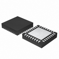
MCU 3V 16K 32-QFN
Manufacturer
Renesas Electronics America
Series
H8® H8/300H SLPr
Datasheet
1.DF38602RFT10.pdf
(554 pages)
Specifications of DF38602RFT10
Core Processor
H8/300H
Core Size
16-Bit
Speed
10MHz
Connectivity
I²C, IrDA, SCI, SSU
Peripherals
POR, PWM, WDT
Number Of I /o
13
Program Memory Size
16KB (16K x 8)
Program Memory Type
FLASH
Ram Size
1K x 8
Voltage - Supply (vcc/vdd)
2.7 V ~ 3.6 V
Data Converters
A/D 6x10b
Oscillator Type
Internal
Operating Temperature
-20°C ~ 75°C
Package / Case
32-QFN
Lead Free Status / RoHS Status
Contains lead / RoHS non-compliant
Eeprom Size
-
Other names
HD64F38602RFT10
HD64F38602RFT10
HD64F38602RFT10
Available stocks
Company
Part Number
Manufacturer
Quantity
Price
Company:

Part Number:
DF38602RFT10V
Manufacturer:
Renesas Electronics America
Quantity:
135


Figure 10.10 PWM Mode Example (2) ...................................................................................... 171
Figure 10.11 Buffer Operation Example (Output Compare) ...................................................... 172
Figure 10.12 PWM Mode Example
Figure 10.13 PWM Mode Example
Figure 10.14 Count Timing for Internal Clock Source ............................................................... 175
Figure 10.15 Count Timing for External Clock Source.............................................................. 175
Figure 10.16 Output Compare Output Timing ........................................................................... 176
Figure 10.17 Input Capture Input Signal Timing........................................................................ 177
Figure 10.18 Timing of Counter Clearing by Compare Match................................................... 177
Figure 10.19 Buffer Operation Timing (Compare Match).......................................................... 178
Figure 10.20 Buffer Operation Timing (Input Capture) ............................................................. 178
Figure 10.21 Timing of IMFA to IMFD Flag Setting at Compare Match .................................. 179
Figure 10.22 Timing of IMFA to IMFD Flag Setting at Input Capture...................................... 180
Figure 10.23 Timing of Status Flag Clearing by CPU................................................................ 180
Figure 10.24 Contention between TCNT Write and Clear ......................................................... 183
Figure 10.25 Internal Clock Switching and TCNT Operation.................................................... 183
Section 11 Realtime Clock (RTC)
Figure 11.1 Block Diagram of RTC ........................................................................................... 186
Figure 11.2 Definition of Time Expression ................................................................................ 191
Figure 11.3 Initial Setting Procedure .......................................................................................... 196
Figure 11.4 Example: Reading of Inaccurate Time Data............................................................ 197
Section 12 Watchdog Timer
Figure 12.1 Block Diagram of Watchdog Timer ........................................................................ 202
Figure 12.2 Example of Watchdog Timer Operation.................................................................. 208
Figure 12.3 Interval Timer Mode Operation............................................................................... 209
Figure 12.4 Timing of OVF Flag Setting.................................................................................... 209
Section 13 Asynchronous Event Counter (AEC)
Figure 13.1 Block Diagram of Asynchronous Event Counter .................................................... 214
Figure 13.2 Software Procedure when Using ECH and ECL as 16-Bit Event Counter.............. 223
Figure 13.3 Software Procedure when Using ECH and ECL as 8-Bit Event Counters .............. 224
Figure 13.4 Event Counter Operation Waveform....................................................................... 226
Figure 13.5 Example of Clock Control Operation...................................................................... 227
Section 14 Serial Communication Interface 3 (SCI3, IrDA)
Figure 14.1 Block Diagram of SCI3 ........................................................................................... 232
Figure 14.2 Data Format in Asynchronous Communication ...................................................... 254
(TOB, TOC, and TOD = 0: initial output values are set to 0)............................... 173
(TOB, TOC, and TOD = 1: initial output values are set to 1)............................... 174
Rev. 3.00 May 15, 2007 Page xxiii of xxxii
Related parts for DF38602RFT10
Image
Part Number
Description
Manufacturer
Datasheet
Request
R

Part Number:
Description:
KIT STARTER FOR M16C/29
Manufacturer:
Renesas Electronics America
Datasheet:

Part Number:
Description:
KIT STARTER FOR R8C/2D
Manufacturer:
Renesas Electronics America
Datasheet:

Part Number:
Description:
R0K33062P STARTER KIT
Manufacturer:
Renesas Electronics America
Datasheet:

Part Number:
Description:
KIT STARTER FOR R8C/23 E8A
Manufacturer:
Renesas Electronics America
Datasheet:

Part Number:
Description:
KIT STARTER FOR R8C/25
Manufacturer:
Renesas Electronics America
Datasheet:

Part Number:
Description:
KIT STARTER H8S2456 SHARPE DSPLY
Manufacturer:
Renesas Electronics America
Datasheet:

Part Number:
Description:
KIT STARTER FOR R8C38C
Manufacturer:
Renesas Electronics America
Datasheet:

Part Number:
Description:
KIT STARTER FOR R8C35C
Manufacturer:
Renesas Electronics America
Datasheet:

Part Number:
Description:
KIT STARTER FOR R8CL3AC+LCD APPS
Manufacturer:
Renesas Electronics America
Datasheet:
Part Number:
Description:
KIT STARTER FOR RX610
Manufacturer:
Renesas Electronics America
Datasheet:

Part Number:
Description:
KIT STARTER FOR R32C/118
Manufacturer:
Renesas Electronics America
Datasheet:

Part Number:
Description:
KIT DEV RSK-R8C/26-29
Manufacturer:
Renesas Electronics America
Datasheet:

Part Number:
Description:
KIT STARTER FOR SH7124
Manufacturer:
Renesas Electronics America
Datasheet:

Part Number:
Description:
KIT STARTER FOR H8SX/1622
Manufacturer:
Renesas Electronics America
Datasheet:

Part Number:
Description:
KIT DEV FOR SH7203
Manufacturer:
Renesas Electronics America
Datasheet: