DF38602RFT10 Renesas Electronics America, DF38602RFT10 Datasheet - Page 26
DF38602RFT10
Manufacturer Part Number
DF38602RFT10
Description
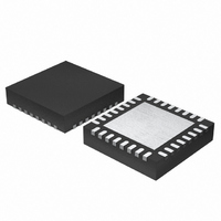
MCU 3V 16K 32-QFN
Manufacturer
Renesas Electronics America
Series
H8® H8/300H SLPr
Datasheet
1.DF38602RFT10.pdf
(554 pages)
Specifications of DF38602RFT10
Core Processor
H8/300H
Core Size
16-Bit
Speed
10MHz
Connectivity
I²C, IrDA, SCI, SSU
Peripherals
POR, PWM, WDT
Number Of I /o
13
Program Memory Size
16KB (16K x 8)
Program Memory Type
FLASH
Ram Size
1K x 8
Voltage - Supply (vcc/vdd)
2.7 V ~ 3.6 V
Data Converters
A/D 6x10b
Oscillator Type
Internal
Operating Temperature
-20°C ~ 75°C
Package / Case
32-QFN
Lead Free Status / RoHS Status
Contains lead / RoHS non-compliant
Eeprom Size
-
Other names
HD64F38602RFT10
HD64F38602RFT10
HD64F38602RFT10
Available stocks
Company
Part Number
Manufacturer
Quantity
Price
Company:

Part Number:
DF38602RFT10V
Manufacturer:
Renesas Electronics America
Quantity:
135


Figure 14.3 Relationship between Output Clock and Transfer Data Phase
Figure 14.4 Sample SCI3 Initialization Flowchart ..................................................................... 258
Figure 14.5 Example SCI3 Operation in Transmission in Asynchronous Mode
Figure 14.6 Sample Serial Transmission Flowchart (Asynchronous Mode) .............................. 260
Figure 14.7 Example SCI3 Operation in Reception in Asynchronous Mode
Figure 14.8 Sample Serial Data Reception Flowchart (Asynchronous Mode) (1) ..................... 263
Figure 14.8 Sample Serial Data Reception Flowchart (Asynchronous Mode) (2) ..................... 264
Figure 14.9 Data Format in Clock Synchronous Communication.............................................. 265
Figure 14.10 Example of SCI3 Operation in Transmission in
Figure 14.11 Sample Serial Transmission Flowchart (Clock Synchronous Mode) .................... 267
Figure 14.12 Example of SCI3 Reception Operation in Clock Synchronous Mode................... 268
Figure 14.13 Sample Serial Reception Flowchart (Clock Synchronous Mode) ......................... 269
Figure 14.14 Sample Flowchart of Simultaneous Serial Transmit and
Figure 14.15 IrDA Block Diagram............................................................................................. 271
Figure 14.16 IrDA Transmission and Reception ........................................................................ 272
Figure 14.17 (a) RDRF Setting and RXI Interrupt ..................................................................... 276
Figure 14.17 (b) TDRE Setting and TXI Interrupt ..................................................................... 276
Figure 14.17 (c) TEND Setting and TEI Interrupt...................................................................... 276
Figure 14.18 Receive Data Sampling Timing in Asynchronous Mode ...................................... 278
Figure 14.19 Relation between RDR Read Timing and Data..................................................... 280
Section 15 Synchronous Serial Communication Unit (SSU)
Figure 15.1 Block Diagram of SSU............................................................................................ 284
Figure 15.2 Relationship between Clock Polarity and Phase, and Data ..................................... 294
Figure 15.3 Relationship between Data Input/Output Pin and Shift Register ............................ 295
Figure 15.4 Initialization in Clocked Synchronous Communication Mode................................ 297
Figure 15.5 Example of Operation in Data Transmission .......................................................... 298
Figure 15.6 Sample Serial Transmission Flowchart ................................................................... 299
Figure 15.7 Example of Operation in Data Reception (MSS = 1) .............................................. 300
Figure 15.8 Sample Serial Reception Flowchart (MSS = 1)....................................................... 301
Figure 15.9 Sample Flowchart for Serial Transmit and Receive Operations.............................. 302
Figure 15.10 Initialization in Four-Line Bus Communication Mode ......................................... 304
Figure 15.11 Example of Operation in Data Transmission (MSS = 1)....................................... 306
Figure 15.12 Example of Operation in Data Reception (MSS = 1) ............................................ 308
Figure 15.13 Arbitration Check Timing ..................................................................................... 309
Rev. 3.00 May 15, 2007 Page xxiv of xxxii
(Asynchronous Mode) (Example with 8-Bit Data, Parity, Two Stop Bits) ............ 254
(8-Bit Data, Parity, One Stop Bit)........................................................................... 259
(8-Bit Data, Parity, One Stop Bit)........................................................................... 262
Clock Synchronous Mode ..................................................................................... 266
Receive Operations (Clock Synchronous Mode) .................................................. 270
Related parts for DF38602RFT10
Image
Part Number
Description
Manufacturer
Datasheet
Request
R

Part Number:
Description:
KIT STARTER FOR M16C/29
Manufacturer:
Renesas Electronics America
Datasheet:

Part Number:
Description:
KIT STARTER FOR R8C/2D
Manufacturer:
Renesas Electronics America
Datasheet:

Part Number:
Description:
R0K33062P STARTER KIT
Manufacturer:
Renesas Electronics America
Datasheet:

Part Number:
Description:
KIT STARTER FOR R8C/23 E8A
Manufacturer:
Renesas Electronics America
Datasheet:

Part Number:
Description:
KIT STARTER FOR R8C/25
Manufacturer:
Renesas Electronics America
Datasheet:

Part Number:
Description:
KIT STARTER H8S2456 SHARPE DSPLY
Manufacturer:
Renesas Electronics America
Datasheet:

Part Number:
Description:
KIT STARTER FOR R8C38C
Manufacturer:
Renesas Electronics America
Datasheet:

Part Number:
Description:
KIT STARTER FOR R8C35C
Manufacturer:
Renesas Electronics America
Datasheet:

Part Number:
Description:
KIT STARTER FOR R8CL3AC+LCD APPS
Manufacturer:
Renesas Electronics America
Datasheet:
Part Number:
Description:
KIT STARTER FOR RX610
Manufacturer:
Renesas Electronics America
Datasheet:

Part Number:
Description:
KIT STARTER FOR R32C/118
Manufacturer:
Renesas Electronics America
Datasheet:

Part Number:
Description:
KIT DEV RSK-R8C/26-29
Manufacturer:
Renesas Electronics America
Datasheet:

Part Number:
Description:
KIT STARTER FOR SH7124
Manufacturer:
Renesas Electronics America
Datasheet:

Part Number:
Description:
KIT STARTER FOR H8SX/1622
Manufacturer:
Renesas Electronics America
Datasheet:

Part Number:
Description:
KIT DEV FOR SH7203
Manufacturer:
Renesas Electronics America
Datasheet: