DF38602RFT10 Renesas Electronics America, DF38602RFT10 Datasheet - Page 542
DF38602RFT10
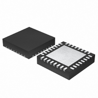
Manufacturer Part Number
DF38602RFT10
Description
MCU 3V 16K 32-QFN
Manufacturer
Renesas Electronics America
Series
H8® H8/300H SLPr
Datasheet
1.DF38602RFT10.pdf
(554 pages)
Specifications of DF38602RFT10
Core Processor
H8/300H
Core Size
16-Bit
Speed
10MHz
Connectivity
I²C, IrDA, SCI, SSU
Peripherals
POR, PWM, WDT
Number Of I /o
13
Program Memory Size
16KB (16K x 8)
Program Memory Type
FLASH
Ram Size
1K x 8
Voltage - Supply (vcc/vdd)
2.7 V ~ 3.6 V
Data Converters
A/D 6x10b
Oscillator Type
Internal
Operating Temperature
-20°C ~ 75°C
Package / Case
32-QFN
Lead Free Status / RoHS Status
Contains lead / RoHS non-compliant
Eeprom Size
-
Other names
HD64F38602RFT10
HD64F38602RFT10
HD64F38602RFT10
Available stocks
Company
Part Number
Manufacturer
Quantity
Price
Company:

Part Number:
DF38602RFT10V
Manufacturer:
Renesas Electronics America
Quantity:
135


Rev. 3.00 May 15, 2007 Page 508 of 516
REJ09B0152-0300
Item
14.8.2 Mark State and Break
Sending
Section 16 I2C Bus Interface 2
(IIC2)
16.3.5 I
(ICSR)
2
C Bus Status Register
Page Revisions (See Manual for Details)
277
323
Modified
When the SPC3 bit in SPCR is 0, the TXD3 pin
functions as an I/O port whose direction (input or
output) and level are determined by PCR and PDR,
regardless of the TE setting. This can be used to set the
TXD3 pin to the mark state (high level) or send a break
during data transmission. To maintain the
communication line at the mark state until the SPC3 bit
in SPCR is set to 1, set both PCR and PDR to 1. As the
SPC3 bit in SPCR is cleared to 0 at this point, the TXD3
pin functions as an I/O port, and 1 is output from the
TXD3 pin. To send a break during data transmission,
first set PCR to 1 and PDR to 0, and then clear the
SPC3 and TE bits to 0. When the TE bit is cleared to 0
directly after the SPC3 bit is cleared to 0, the transmitter
is initialized regardless of the current transmission state
after the TE bit is cleared, the TXD3 pin functions as an
I/O port after the SPC3 bit is cleared, and 0 is output
from the TXD3 pin.
Modified
Bit
3
Bit Name
STOP
Description
Stop Condition Detection Flag[Setting
conditions]
•
•
In master mode, when a stop condition
is detected after the completion of
frame transfer
In slave mode, when a stop condition is
detected, after the slave address of the
first byte, following the general call and
the detection of the start condition,
matches the address set in SAR
Related parts for DF38602RFT10
Image
Part Number
Description
Manufacturer
Datasheet
Request
R

Part Number:
Description:
KIT STARTER FOR M16C/29
Manufacturer:
Renesas Electronics America
Datasheet:

Part Number:
Description:
KIT STARTER FOR R8C/2D
Manufacturer:
Renesas Electronics America
Datasheet:

Part Number:
Description:
R0K33062P STARTER KIT
Manufacturer:
Renesas Electronics America
Datasheet:

Part Number:
Description:
KIT STARTER FOR R8C/23 E8A
Manufacturer:
Renesas Electronics America
Datasheet:

Part Number:
Description:
KIT STARTER FOR R8C/25
Manufacturer:
Renesas Electronics America
Datasheet:

Part Number:
Description:
KIT STARTER H8S2456 SHARPE DSPLY
Manufacturer:
Renesas Electronics America
Datasheet:

Part Number:
Description:
KIT STARTER FOR R8C38C
Manufacturer:
Renesas Electronics America
Datasheet:

Part Number:
Description:
KIT STARTER FOR R8C35C
Manufacturer:
Renesas Electronics America
Datasheet:

Part Number:
Description:
KIT STARTER FOR R8CL3AC+LCD APPS
Manufacturer:
Renesas Electronics America
Datasheet:
Part Number:
Description:
KIT STARTER FOR RX610
Manufacturer:
Renesas Electronics America
Datasheet:

Part Number:
Description:
KIT STARTER FOR R32C/118
Manufacturer:
Renesas Electronics America
Datasheet:

Part Number:
Description:
KIT DEV RSK-R8C/26-29
Manufacturer:
Renesas Electronics America
Datasheet:

Part Number:
Description:
KIT STARTER FOR SH7124
Manufacturer:
Renesas Electronics America
Datasheet:

Part Number:
Description:
KIT STARTER FOR H8SX/1622
Manufacturer:
Renesas Electronics America
Datasheet:

Part Number:
Description:
KIT DEV FOR SH7203
Manufacturer:
Renesas Electronics America
Datasheet: