M30624FGNGP#D5 Renesas Electronics America, M30624FGNGP#D5 Datasheet
M30624FGNGP#D5
Specifications of M30624FGNGP#D5
Available stocks


Related parts for M30624FGNGP#D5


M30624FGNGP#D5 Summary of contents
Page 1
To our customers, Old Company Name in Catalogs and Other Documents st On April 1 , 2010, NEC Electronics Corporation merged with Renesas Technology Corporation, and Renesas Electronics Corporation took over all the business of both companies. Therefore, although the ...
Page 2
All information included in this document is current as of the date this document is issued. Such information, however, is subject to change without any prior notice. Before purchasing or using any Renesas Electronics products listed herein, please confirm ...
Page 3
To all our customers Regarding the change of names mentioned in the document, such as Mitsubishi Electric and Mitsubishi XX, to Renesas Technology Corp. The semiconductor operations of Hitachi and Mitsubishi Electric were transferred to Renesas Technology Corporation on April ...
Page 4
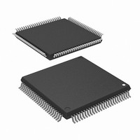
Rev.1.1 Description Description The M16C/62N group of single-chip microcomputers are built using the high-performance silicon gate CMOS process using a M16C/60 Series CPU core and are packaged in a 100-pin plastic molded QFP. These single-chip microcomputers operate using sophisticated instructions ...
Page 5
Description Pin Configuration Figures 1.1.1 and 1.1.2 show the pin configurations (top view). PIN CONFIGURATION (top view / / /AN /D ...
Page 6
Description Mitsubishi microcomputers M16C / 62N Group SINGLE-CHIP 16-BIT CMOS MICROCOMPUTER 3 ...
Page 7
Description Block Diagram Figure 1.1 block diagram of the M16C/62N group. 8 I/O ports Port P0 Internal peripheral functions Timer Timer TA0 (16 bits) Timer TA1 (16 bits) Timer TA2 (16 bits) Timer TA3 (16 bits) Timer TA4 ...
Page 8
Description Performance Outline Table 1.1 performance outline of M16C/62N group. Table 1.1.1. Performance outline of M16C/62N group Item Number of basic instructions Shortest instruction execution time Memory ROM capacity RAM I/O port P0 to P10 (except P8 Input ...
Page 9
Description Mitsubishi plans to release the following products in the M16C/62N group: (1) Support for mask ROM version and flash memory version (2) ROM capacity (3) Package 100P6S-A : Plastic molded QFP (mask ROM and flash memory versions) 100P6Q-A : ...
Page 10
Description Type No N– Figure 1.1.5. Type No., memory size, and package Mitsubishi microcomputers M16C / 62N Group SINGLE-CHIP 16-BIT CMOS MICROCOMPUTER Package type Package ...
Page 11
Pin Description Pin Description Pin name Signal name Power supply input CNV CNV Input SS SS RESET Reset input Input X Clock input Input IN X Clock output Output OUT BYTE External data Input bus ...
Page 12
Pin Description Pin Description Pin name Signal name I/O port P5 Input/output 0 7 Output WRL / WR, Output WRH / BHE, Output RD, Output BCLK, Output HLDA, Input HOLD, ALE, Output RDY Input ...
Page 13
Memory Operation of Functional Blocks The M16C/62N group accommodates certain units in a single chip. These units include ROM and RAM to store instructions and data and the central processing unit (CPU) to execute arithmetic/logic operations. Also included are peripheral ...
Page 14
CPU Central Processing Unit (CPU) The CPU has a total of 13 registers shown in Figure 1.4.1. Seven of these registers (R0, R1, R2, R3, A0, A1, and FB) come in two sets; therefore, these have two register banks. b15 ...
Page 15
CPU (3) Frame base register (FB) Frame base register (FB) is configured with 16 bits, and is used for FB relative addressing. (4) Program counter (PC) Program counter (PC) is configured with 20 bits, indicating the address of an instruction ...
Page 16
CPU • Bit 7: Stack pointer select flag (U flag) Interrupt stack pointer (ISP) is selected when this flag is “0” ; user stack pointer (USP) is selected when this flag is “1”. This flag is cleared to “0” when ...
Page 17
Reset Reset There are two kinds of resets; hardware and software. In both cases, operation is the same after the reset. (See “Software Reset” for details of software resets.) This section explains on hardware resets. When the supply voltage is ...
Page 18
Reset Table 1.5.1 shows the statuses of the other pins while the RESET pin level is “L”. Figures 1.5.3 and 1.5.4 show the internal status of the microcomputer immediately after the reset is cancelled. Table 1.5.1. Pin status when RESET ...
Page 19
Reset (1) Processor mode register 0 (Note) (2) Processor mode register 1 (3) System clock control register 0 (4) System clock control register 1 (5) Chip select control register (6) Address match interrupt enable register (7) Protect register (8) Data ...
Page 20
Reset (59) Count start flag (60) Clock prescaler reset flag (61) One-shot start flag (62) Trigger select flag (63) Up-down flag (64) Timer A0 mode register (65) Timer A1 mode register (66) Timer A2 mode register (67) Timer A3 mode ...
Page 21
SFR 0000 16 0001 16 0002 16 0003 16 Processor mode register 0 (PM0) 0004 16 Processor mode register 1(PM1) 0005 16 System clock control register 0 (CM0) 0006 16 System clock control register 1 (CM1) 0007 16 Chip select ...
Page 22
SFR 0340 Timer B3 count start flag (TBSR) 16 0341 16 0342 16 Timer A1-1 register (TA11) 0343 16 0344 16 Timer A2-1 register (TA21) 0345 16 0346 16 Timer A4-1 register (TA41) 0347 16 Three-phase PWM control ...
Page 23
SFR 03C0 16 03C1 16 03C2 16 03C3 16 03C4 16 03C5 16 03C6 16 03C7 16 03C8 16 03C9 16 03CA 16 03CB 16 03CC 16 03CD 16 03CE 16 03CF 16 03D0 16 03D1 16 03D2 16 03D3 ...
Page 24
Memory Space Expansion Features Memory Space Expansion Features Here follows the description of the memory space expansion features. With the processor running in memory expansion mode or in microprocessor mode, the memory space expansion features provide the means of expanding ...
Page 25
Memory Space Expansion Features (2) Expansion mode In expansion mode, the data bank register (0000B register. Data bank register Figure 1.7.2. Data bank register Expansion mode (memory space = 4M bytes for ...
Page 26
Memory Space Expansion Features The data bank register is made up of the bank selection bits (bits 5 through 3) and the offset bit (bit 2). The bank selection bits are used to set a bank number for accessing data ...
Page 27
Memory Space Expansion Features Areas used for data only 000000 16 to 380000 16 Area commonly used for data and programs 380000 to 3BFFFF 16 16 Area commonly used for data and programs 3C0000 to 3FFFFF 16 16 Figure 1.7.5. ...
Page 28
Software Reset Software Reset Software Reset Writing “1” to bit 3 of the processor mode register 0 (address 0004 microcomputer. A software reset has the same effect as a hardware reset. The contents of internal RAM are preserved. Processor Mode ...
Page 29
Processor Mode Figure 1.8.1 shows the processor mode register 0 and 1. Figure 1.8.2 shows the memory maps in each processor mode (without memory area expansion, normal mode). Processor mode register 0 (Note 1) Symbol ...
Page 30
Processor Mode Single-chip mode 00000 16 SFR area 00400 16 Internal RAM area XXXXX 16 04000 16 Inhibited D0000 16 YYYYY 16 Internal ROM area FFFFF 16 Address XXXXX RAM size 16 10K bytes 02BFF 16 12K bytes 033FF 16 ...
Page 31
Processor Mode Figure 1.8.3 shows the memory maps and the chip selection areas effected by PM13 (the internal re- served area expansion bit) in each processor mode for the product having an internal RAM of more than 15K bytes and ...
Page 32
Bus Settings Bus Settings The BYTE pin and bits the processor mode register 0 (address 0004 Table 1.9.1 shows the factors used to change the bus settings. Table 1.9.1. Factors for switching bus settings Bus setting ...
Page 33
Bus Settings Table 1.9.2. Pin functions for each processor mode Single-chip Processor mode mode Multiplexed bus space select bit Data bus width BYTE pin level I/O port I/O port ...
Page 34
Bus Control Bus Control The following explains the signals required for accessing external devices and software waits. The signals required for accessing the external devices are valid when the processor mode is set to memory expansion mode and microprocessor mode. ...
Page 35
Bus Control Table 1.10.2. External areas specified by the chip select signals (A product having an internal RAM of more than 15K bytes and a ROM of more than 192K bytes) Memory space Processor mode expansion mode Memory expansion mode ...
Page 36
Bus Control Example 1) After access the external area, both the address signal and the chip select signal change concurrently in the next cycle. In this example, after access to the external area(i), an access to the area indicated by ...
Page 37
Bus Control (3) Read/write signals With a 16-bit data bus (BYTE pin =“L”), bit 2 of the processor mode register 0 (address 0004 _____ ________ combinations of RD, BHE, and WR signals or RD, WRL, and WRH signals. With an ...
Page 38
Bus Control ________ (5) The RDY signal ________ RDY is a signal that facilitates access to an external device that requires long access time. As shown in Figure 1.10. “L” is being input to the RDY at the ...
Page 39
Bus Control (6) Hold signal The hold signal is used to transfer the bus privileges from the CPU to the external circuits. Inputting “L” to __________ the HOLD pin places the microcomputer in the hold state at the end of ...
Page 40
Bus Control (8) BCLK output The user can choose the BCLK output by use of bit 7 of processor mode register 0 (0004 When set to “1”, the output floating. Note: Before attempting to change the contents of the processor ...
Page 41
Bus Control < Separate bus (no wait) > BCLK Write signal Read signal Data bus Address bus (Note 2) Chip select (Note 2) < Separate bus (with wait) > BCLK Write signal Read signal Data bus Address bus (Note 2) ...
Page 42
Clock Generating Circuit Clock Generating Circuit The clock generating circuit contains two oscillator circuits that supply the operating clock sources to the CPU and internal peripheral units. Table 1.11.1. Main clock and sub-clock generating circuits Use of clock Usable oscillator ...
Page 43
Clock Generating Circuit Clock Control Figure 1.11.3 shows the block diagram of the clock generating circuit. CM10 “1” Write signal RESET Software reset NMI Interrupt request level judgment output WAIT instruction CM0i : Bit i at address 0006 CM1i : ...
Page 44
Clock Generating Circuit The following paragraphs describes the clocks generated by the clock generating circuit. (1) Main clock The main clock is generated by the main clock oscillation circuit. After a reset, the clock is divided the ...
Page 45
Clock Generating Circuit Figure 1.11.4 shows the system clock control registers 0 and 1. System clock control register 0 (Note Symbol CM0 Bit symbol CM00 CM01 CM02 CM03 CM04 CM05 CM06 ...
Page 46
Clock Generating Circuit Clock Output In single-chip mode, the clock output function select bits (bits 0 and 1 at address 0006 output from the P5 /CLK 7 0006 ) is set to “1”, the output of f ...
Page 47
Wait Mode Wait Mode When a WAIT instruction is executed, the BCLK stops and the microcomputer enters the wait mode. In this mode, oscillation continues but the BCLK and watchdog timer stop. Writing “1” to the WAIT peripheral function clock ...
Page 48
Status Transition of BCLK Status Transition of BCLK Power dissipation can be reduced and low-voltage operation achieved by changing the count source for BCLK. Table 1.11.4 shows the operating modes corresponding to the settings of system clock control registers 0 ...
Page 49
Power control Power control The following is a description of the three available power control modes: Modes Power control is available in three modes. (a) Normal operation mode • High-speed mode Divide-by-1 frequency of the main clock becomes the BCLK. ...
Page 50
Power control Transition of stop mode, wait mode All oscillators stopped Stop mode CM07 = “0” CM06 = “1” CM05 = “0” CM10 = “1” (Note) All oscillators stopped Stop mode All oscillators stopped Stop mode Transition of normal mode ...
Page 51
Protection Protection The protection function is provided so that the values in important registers cannot be changed in the event that the program runs out of control. Figure 1.11.6 shows the protect register. The values in the processor mode register ...
Page 52
Interrupt Overview of Interrupt Type of Interrupts Figure 1.12.1 lists the types of interrupts. Software Interrupt Hardware Note: Peripheral I/O interrupts are generated by the peripheral functions built into the microcomputer system. Figure 1.12.1. Classification of interrupts • Maskable interrupt ...
Page 53
Interrupt Software Interrupts A software interrupt occurs when executing certain instructions. Software interrupts are non-maskable interrupts. • Undefined instruction interrupt An undefined instruction interrupt occurs when executing the UND instruction. • Overflow interrupt An overflow interrupt occurs when executing the ...
Page 54
Interrupt Hardware Interrupts Hardware interrupts are classified into two types — special interrupts and peripheral I/O interrupts. (1) Special interrupts Special interrupts are non-maskable interrupts. • Reset Reset occurs if an “L” is input to the RESET pin. _______ • ...
Page 55
Interrupt Interrupts and Interrupt Vector Tables If an interrupt request is accepted, a program branches to the interrupt routine set in the interrupt vector table. Set the first address of the interrupt routine in each vector table. Figure 1.12.2 shows ...
Page 56
Interrupt • Variable vector tables The addresses in the variable vector table can be modified, according to the user’s settings. Indicate the first address using the interrupt table register (INTB). The 256-byte area subsequent to the ad- dress the INTB ...
Page 57
Interrupt Interrupt Control Descriptions are given here regarding how to enable or disable maskable interrupts and how to set the priority to be accepted. What is described here does not apply to non-maskable interrupts. Enable or disable a maskable interrupt ...
Page 58
Interrupt Interrupt control register (Note Bit symbol Nothing is assigned attempt to write to these bits, write “0”. The value, if read, turns out to be indeterminate. Note 1: ...
Page 59
Interrupt Interrupt Enable Flag (I flag) The interrupt enable flag (I flag) controls the enabling and disabling of maskable interrupts. Setting this flag to “1” enables all maskable interrupts; setting it to “0” disables all maskable interrupts. This flag is ...
Page 60
Interrupt Rewrite the interrupt control register To rewrite the interrupt control register point that does not generate the interrupt request for that register. If there is possibility of the interrupt request occur, rewrite the interrupt control ...
Page 61
Interrupt Interrupt Sequence An interrupt sequence — what are performed over a period from the instant an interrupt is accepted to the instant the interrupt routine is executed — is described here interrupt occurs during execution of an ...
Page 62
Interrupt Time (a) is dependent on the instruction under execution. Thirty cycles is the maximum required for the DIVX instruction (without wait). Time ( shown in Table 1.12.5. Table 1.12.5. Time required for executing the interrupt sequence Interrupt ...
Page 63
Interrupt Saving Registers In the interrupt sequence, only the contents of the flag register (FLG) and that of the program counter (PC) are saved in the stack area. First, the processor saves the four higher-order bits of the program counter, ...
Page 64
Interrupt The operation of saving registers carried out in the interrupt sequence is dependent on whether the content of the stack pointer (Note the time of acceptance of an interrupt request, is even or odd. If the content ...
Page 65
Interrupt Returning from an Interrupt Routine Executing the REIT instruction at the end of an interrupt routine returns the contents of the flag register (FLG was immediately before the start of interrupt sequence and the contents of the ...
Page 66
Interrupt Priority level of each interrupt INT1 Timer B2 Timer B0 Timer A3 Timer A1 Timer B4 INT3 INT2 INT0 Timer B1 Timer A4 Timer A2 Timer B3 Timer B5 UART1 reception UART0 reception UART2 reception/ACK A-D conversion DMA1 Bus ...
Page 67
INT Interrupt ______ INT Interrupt ________ ________ INT0 to INT5 are triggered by the edges of external inputs. The edge polarity is selected using the polarity select bit. Of interrupt control registers, 0048 register, and 0049 is used both ...
Page 68
NMI Interrupt ______ NMI Interrupt ______ An NMI interrupt is generated when the input to the non-maskable external interrupt. The pin level can be checked in the port P8 03F0 ). 16 This pin cannot be ...
Page 69
Address Match Interrupt Address Match Interrupt An address match interrupt is generated when the address match interrupt address register contents match the program counter value. Two address match interrupts can be set, each of which can be enabled and disabled ...
Page 70
Precautions for Interrupts Precautions for Interrupts (1) Reading address 00000 • When maskable interrupt is occurred, CPU reads the interrupt information (the interrupt number and interrupt request level) in the interrupt sequence. The interrupt request bit of the certain interrupt ...
Page 71
Precautions for Interrupts Figure 1.12.13. Switching condition of INT interrupt request (6) Rewrite the interrupt control register • To rewrite the interrupt control register point that does not generate the interrupt request for that register. If ...
Page 72
Watchdog Timer Watchdog Timer The watchdog timer has the function of detecting when the program is out of control. Therefore, we recom- mend using the watchdog timer to improve reliability of a system. The watchdog timer is a 15-bit counter ...
Page 73
Watchdog Timer Prescaler BCLK HOLD Write to the watchdog timer start register (address 000E ) 16 RESET Figure 1.13.1. Block diagram of watchdog timer Watchdog timer control register Watchdog timer ...
Page 74
DMAC DMAC This microcomputer has two DMAC (direct memory access controller) channels that allow data to be sent to memory without using the CPU. DMAC shares the same data bus with the CPU. The DMAC is given a higher right ...
Page 75
DMAC Table 1.14.1. DMAC specifications Item No. of channels Transfer memory space Maximum No. of bytes transferred DMA request factors (Note) Channel priority Transfer unit Transfer address direction Transfer mode DMA interrupt request generation timing When an underflow occurs in ...
Page 76
DMAC DMA0 request cause select register Figure 1.14.2. DMAC register (1) SINGLE-CHIP 16-BIT CMOS MICROCOMPUTER Symbol Address b0 DM0SL 03B8 16 Bit name Bit symbol DMA request cause DSEL0 ...
Page 77
DMAC DMA1 request cause select register Bit symbol DSEL0 DSEL1 DSEL2 DSEL3 Nothing is assigned attempt to write to these bits, write “0”. The value, if read, turns out to ...
Page 78
DMAC DMAi source pointer ( (b19) (b16)(b15) (b23 DMAi destination pointer ( (b19) (b16) (b15) (b23 DMAi transfer counter ( (b15) (b8) b7 ...
Page 79
DMAC (1) Transfer cycle The transfer cycle consists of the bus cycle in which data is read from memory or from the SFR area (source read) and the bus cycle in which the data is written to memory or to ...
Page 80
DMAC (1) 8-bit transfers 16-bit transfers and the source address is even. BCLK Address CPU use bus RD signal WR signal Data CPU use bus (2) 16-bit transfers and the source address is odd Transferring 16-bit data on an 8-bit ...
Page 81
DMAC (2) DMAC transfer cycles Any combination of even or odd transfer read and write addresses is possible. Table 1.14.2 shows the number of DMAC transfer cycles. The number of DMAC transfer cycles can be calculated as follows: No. of ...
Page 82
DMAC DMA enable bit Setting the DMA enable bit to “1” makes the DMAC active. The DMAC carries out the following operations at the time data transfer starts immediately after DMAC is turned active. (1) Reloads the value of one ...
Page 83
DMAC (3) The priorities of channels and DMA transfer timing If a DMA transfer request signal falls on a single sampling cycle (a sampling cycle means one period from the leading edge to the trailing edge of BCLK), the DMA ...
Page 84
Timer Timer There are eleven 16-bit timers. These timers can be classified by function into timers A (five) and timers B (six). All these timers function independently. Figures 1.15.1 and 1.15.2 show the block diagram of timers 1/8 ...
Page 85
Timer C32 Noise TB0 IN filter Noise TB1 IN filter Noise TB2 IN filter Noise TB3 IN filter Noise TB4 IN filter Noise TB5 IN filter Note 1: The TB5 ...
Page 86
Timer A Timer A Figure 1.15.3 shows the block diagram of timer A. Figures 1.15.4 to 1.15.6 show the timer A-related registers. Except in event counter mode, timers A0 through A4 all have the same function. Use the timer Ai ...
Page 87
Timer A Timer Ai register (Note 1) (b15) (b8 • Timer mode • Event counter mode • One-shot timer mode Note 1: Read and write data in 16-bit units. Note 2: When the timer Ai register is ...
Page 88
Timer A One-shot start flag Nothing is assigned attempt to write to this bit, write “0”. The value, if read, turns out to be indeterminate. Note: Set the corresponding port ...
Page 89
Timer A (1) Timer mode In this mode, the timer counts an internally generated count source. (See Table 1.15.1.) Figure 1.15.7 shows the timer Ai mode register in timer mode. Table 1.15.1. Specifications of timer mode Item Count source f ...
Page 90
Timer A (2) Event counter mode In this mode, the timer counts an external signal or an internal timer’s overflow. Timers A0 and A1 can count a single-phase external signal. Timers A2, A3, and A4 can count a single-phase and ...
Page 91
Timer A Table 1.15.3. Timer specifications in event counter mode (when processing two-phase pulse signal with timers A2, A3, and A4) Item Count source • Two-phase pulse signals input to TAi Count operation • Up count or down count can ...
Page 92
Timer A Timer Ai mode register (When using two-phase pulse signal processing TMOD0 TMOD1 TCK0 TCK1 Note 1: This bit is valid for timer A3 mode register. ...
Page 93
Timer A (3) One-shot timer mode In this mode, the timer operates only once. (See Table 1.15.4.) When a trigger occurs, the timer starts up and continues operating for a given period. Figure 1.15.10 shows the timer Ai mode register ...
Page 94
Timer A (4) Pulse width modulation (PWM) mode In this mode, the timer outputs pulses of a given width in succession. (See Table 1.15.5.) In this mode, the counter functions as either a 16-bit pulse width modulator or an 8-bit ...
Page 95
Timer A Condition : Reload register = 0003 (rising edge of TA Count source “H” TA pin iIN input signal “L” “H” PWM pulse output from TA pin iOUT “L” Timer Ai interrupt “1” request bit “0” Frequency ...
Page 96
Timer B Timer B Figure 1.15.14 shows the block diagram of timer B. Figures 1.15.15 and 1.15.16 show the timer B-related registers. Use the timer Bi mode register ( bits 0 and 1 to choose the ...
Page 97
Timer B Timer Bi register (Note) (b15) (b8 • Timer mode Counts the timer's period • Event counter mode Counts external pulses input or a timer overflow • Pulse period / pulse width measurement mode Measures a ...
Page 98
Timer B (1) Timer mode In this mode, the timer counts an internally generated count source. (See Table 1.15.6.) Figure 1.15.17 shows the timer Bi mode register in timer mode. Table 1.15.6. Timer specifications in timer mode Item Count source ...
Page 99
Timer B (2) Event counter mode In this mode, the timer counts an external signal or an internal timer's overflow. (See Table 1.15.7.) Figure 1.15.18 shows the timer Bi mode register in event counter mode. Table 1.15.7. Timer specifications in ...
Page 100
Timer B (3) Pulse period/pulse width measurement mode In this mode, the timer measures the pulse period or pulse width of an external signal. (See Table 1.15.8.) Figure 1.15.19 shows the timer Bi mode register in pulse period/pulse width measurement ...
Page 101
Timer B When measuring measurement pulse time interval from falling edge to falling edge Count source “H” Measurement pulse “L” Reload register counter transfer timing Timing at which counter reaches “0000 ” 16 “1” Count start flag “0” “1” Timer ...
Page 102
Timers’ functions for three-phase motor control Timers’ functions for three-phase motor control Use of more than one built-in timer A and timer B provides the means of outputting three-phase motor driving waveforms. Figures 1.16.1 to 1.16.3 show registers related to ...
Page 103
Timers’ functions for three-phase motor control Three-phase output buffer register Bit Symbol DUB0 DVB0 DW0 DWB0 Nothing is assigned attempt to write to these bits, write “0”. The value, ...
Page 104
Timers’ functions for three-phase motor control Timer Ai register (Note 1) (b15) (b8 Timer Ai-1 register (Note) (b15) (b8 Trigger select register Count start flag b7 ...
Page 105
Timers’ functions for three-phase motor control Three-phase motor driving waveform output mode (three-phase PWM output mode) Setting “1” in the mode select bit (bit 2 at 0348 output mode that uses four timers A1, A2, A4, and ...
Page 106
Timers’ functions for three-phase motor control Figure 1.16.5 shows the block diagram for three-phase PWM output mode. In three-phase PWM output mode, the positive-phase waveforms (U phase, V phase, and W phase) and negative waveforms (U ___ ___ phase, V ...
Page 107
Timers’ functions for three-phase motor control Figure 1.16.5. Block diagram for three-phase PWM output mode 104 Mitsubishi microcomputers M16C / 62N Group SINGLE-CHIP 16-BIT CMOS MICROCOMPUTER ...
Page 108
Timers’ functions for three-phase motor control Triangular wave modulation To generate a PWM waveform of triangular wave modulation, set “0” in the modulation mode select bit (bit 6 at 0348 ). Also, set “1” in the timers A4-1, A1-1, A2-1 ...
Page 109
Timers’ functions for three-phase motor control phase waveform. In this way, a waveform can be picked up from the applicable terminal in a manner in which the "L" level of the U phase waveform doesn’t lap over that of the ...
Page 110
Timers’ functions for three-phase motor control Assigning certain values to DU0 (bit 0 at 034A and DUB1 (bit 1 at 034B ) allows the user to output the waveforms as shown in Figure 1.16.7, that is output the ...
Page 111
Timers’ functions for three-phase motor control Sawtooth modulation To generate a PWM waveform of sawtooth wave modulation, set “1” in the modulation mode select bit (bit 6 at 0348 ). Also, set “0” in the timers A4-1, A1-1, and A2-1 ...
Page 112
Timers’ functions for three-phase motor control A carrier wave of sawtooth waveform Carrier wave Signal wave Timer B2 Trigger signal for timer Ai start (timer B2 overflow signal) Timer A4 output m U phase output signal U phase output signal ...
Page 113
Timers’ functions for three-phase motor control A carrier wave of sawtooth waveform Carrier wave Signal wave Timer B2 Interrupt occurs. Rewriting the value of timer A4. Trigger signal for timer Ai start (timer B2 overflow signal) Timer A4 output m ...
Page 114
Serial I/O Serial I/O Serial I/O is configured as five channels: UART0, UART1, UART2, S I/O3 and S I/O4. UART0 to 2 UART0, UART1 and UART2 each have an exclusive timer to generate a transfer clock, so they operate independently ...
Page 115
Serial I/O (UART0) RxD 0 Clock source selection f 1 Internal External Clock synchronous type (when internal clock is selected) CLK polarity CLK 0 reversing circuit CTS/RTS selected CTS / RTS 0 0 Vcc (UART1) RxD ...
Page 116
Serial I/O 1SP SP SP PAR RxDi 2SP PAR 2SP enabled SP SP PAR 1SP Figure 1.17.2. Block diagram of UARTi ( transmit/receive unit Clock synchronous type UART (7 bits) UART (8 bits) Clock ...
Page 117
Serial I/O No reverse RxD data RxD2 reverse circuit Reverse 1SP SP SP PAR 2SP PAR enabled 2SP SP SP PAR 1SP PAR disabled Figure 1.17.3. Block diagram of UART2 transmit/receive unit 114 Clock synchronous type UART ...
Page 118
Serial I/O UARTi transmit buffer register (Note) (b15) (b8 UARTi receive buffer register (b8) (b15 UARTi bit rate generator (Note Figure 1.17.4. Serial I/O-related registers (1) SINGLE-CHIP 16-BIT CMOS MICROCOMPUTER ...
Page 119
Serial I/O UARTi transmit/receive mode register Symbol UiMR(i=0,1) Bit symbol SMD0 Serial I/O mode select bit SMD1 SMD2 CKDIR STPS PRY PRYE SLEP Note : Set the corresponding port direction register to ...
Page 120
Serial I/O UARTi transmit/receive control register UiC0(i=0,1) Bit symbol CLK0 CLK1 CRS TXEPT CRD NCH CKPOL UFORM Transfer format select bit Note 1: Set the corresponding port direction register to “0”. ...
Page 121
Serial I/O UARTi transmit/receive control register Symbol UiC1(i=0,1) Bit symbol Nothing is assigned attempt to write to these bits, write “0”. The value, if read, ...
Page 122
Serial I/O UART transmit/receive control register Symbol 0 UCON Bit symbol U0IRS UART0 transmit interrupt cause select bit U1IRS UART1 transmit interrupt cause select bit U0RRM UART0 continuous receive mode enable ...
Page 123
Serial I/O UART2 special mode register bus exclusive use register Bit symbol IICM2 CSC SWC ALS STAC SWC2 SDHI SHTC UART2 special mode register bus exclusive ...
Page 124
Clock synchronous serial I/O mode (1) Clock synchronous serial I/O mode The clock synchronous serial I/O mode uses a transfer clock to transmit and receive data. Tables 1.17.2 and 1.17.3 list the specifications of the clock synchronous serial I/O mode. ...
Page 125
Clock synchronous serial I/O mode Table 1.17.3. Specifications of clock synchronous serial I/O mode (2) Item Select function • CLK polarity selection Whether transmit data is output/input timing at the rising edge or falling edge of the transfer clock can ...
Page 126
Clock synchronous serial I/O mode UARTi transmit/receive mode registers Bit symbol Note : Set the corresponding port direction register to “0”. UART2 transmit/receive mode register ...
Page 127
Clock synchronous serial I/O mode Table 1.17.4 lists the functions of the input/output pins during clock synchronous serial I/O mode. This table shows the pin functions when the transfer clock output from multiple pins function is not selected. Note that ...
Page 128
Clock synchronous serial I/O mode • Example of transmit timing (when internal clock is selected) Transfer clock “1” Transmit enable “0” Data is set in UARTi transmit buffer register bit (TE) “1” Transmit buffer empty flag (Tl) “0” “H” CTSi ...
Page 129
Clock synchronous serial I/O mode (a) Polarity select function As shown in Figure 1.17.12, the CLK polarity select bit (bit 6 at addresses 03A4 allows selection of the polarity of the transfer clock. • When CLK polarity select bit = ...
Page 130
Clock synchronous serial I/O mode (c) Transfer clock output from multiple pins function (UART1) This function allows the setting two transfer clock output pins and choosing one of the two to output a clock by using the CLK and CLKS ...
Page 131
Clock asynchronous serial I/O (UART) mode (2) Clock asynchronous serial I/O (UART) mode The UART mode allows transmitting and receiving data after setting the desired transfer rate and transfer data format. Tables 1.17.5 and 1.17.6 list the specifications of the ...
Page 132
Clock asynchronous serial I/O (UART) mode Table 1.17.6. Specifications of UART Mode (2) Item Select function • Sleep mode selection (UART0, UART1) This mode is used to transfer data to and from one of multiple slave micro- computers • Serial ...
Page 133
Clock asynchronous serial I/O (UART) mode UARTi transmit / receive mode registers Bit symbol Note : Set the corresponding port direction register to “0”. UART2 transmit / receive mode register b7 b6 ...
Page 134
Clock asynchronous serial I/O (UART) mode Table 1.17.7 lists the functions of the input/output pins during UART mode. Note that for a period from when the UARTi operation mode is selected to when transfer starts, the TxDi pin outputs an ...
Page 135
Clock asynchronous serial I/O (UART) mode • Example of transmit timing when transfer data is 8 bits long (parity enabled, one stop bit) Transfer clock “1” Transmit enable bit(TE) “0” “1” Transmit buffer empty flag(TI) “0” “H” CTSi “L” Start ...
Page 136
Clock asynchronous serial I/O (UART) mode • Example of transmit timing when transfer data is 8 bits long (parity enabled, one stop bit) Transfer clock “1” Transmit enable bit(TE) Data is set in UART2 transmit buffer register “0” Transmit buffer ...
Page 137
Clock asynchronous serial I/O (UART) mode • Example of receive timing when transfer data is 8 bits long (parity disabled, one stop bit) BRGi count source “1” Receive enable bit “0” RxDi Transfer clock Reception triggered when transfer clock “1” ...
Page 138
Clock asynchronous serial I/O (UART) mode (c) TxD, RxD I/O polarity reverse function (UART2) This function is to reverse T (including the start bit, stop bit(s), and parity bit) is reversed. Set this function to “0” (not to reverse) for ...
Page 139
Clock asynchronous serial I/O (UART) mode (3) Clock-asynchronous serial I/O mode (used for the SIM interface) The SIM interface is used for connecting the microcomputer with a memory card or the like; adding some extra settings in UART2 clock-asynchronous serial ...
Page 140
Clock asynchronous serial I/O (UART) mode Transfer clock “1” Transmit enable bit(TE) “0” “1” Transmit buffer empty flag(TI) “0” Start bit TxD RxD 2 Signal conductor level ST D (Note 2) Transmit register “1” empty flag (TXEPT) ...
Page 141
Clock asynchronous serial I/O (UART) mode (a) Function for outputting a parity error signal During reception, with the error signal output enable bit (bit 7 of address 037D can output an “L” level from the T comparing with the case ...
Page 142
Clock asynchronous serial I/O (UART) mode Figure 1.17.25 shows the example of connecting the SIM interface. Connect T pull-up. Figure 1.17.25. Connecting the SIM interface Microcomputer TxD 2 RxD 2 Mitsubishi microcomputers M16C / 62N Group SINGLE-CHIP 16-BIT CMOS MICROCOMPUTER ...
Page 143
UART2 Special Mode Register UART2 Special Mode Register The UART2 special mode register (address 0377 Figure 1.17.26 shows the UART2 special mode register. Bit 0 of the UART2 special mode register (0377 2 Setting “1” in the I C mode ...
Page 144
UART2 Special Mode Register P7 through P7 conforming to the simplified I C bus /TxD /SDA 0 2 Timer I/O Selector SDDS=0 UART2 or DL=000 Digital delay (Divider) SDDS=1 and DL 000 Noize Filter Timer Falling edge ...
Page 145
UART2 Special Mode Register Figure 1.17.27 shows the functional block diagram for I (IICM) causes ports output terminal SCL, and port P7 so the SDA output changes after SCL fully goes to “L”. When digital delay ...
Page 146
UART2 Special Mode Register Some other functions added are explained here. Figure 1.17.28 shows their workings. Bit 4 of the UART2 special mode register is used as the bus collision detect sampling clock select bit. The bus collision detect interrupt ...
Page 147
UART2 Special Mode Register 2 UART2 Special Mode Register 2 UART2 special mode register 2 (address 0376 1.17.29 shows the UART2 special mode register 2. UART2 special mode register bus exclusive use register ...
Page 148
UART2 Special Mode Register 2 Bit 0 of the UART2 special mode register 2 (address 0376 1.17.11 shows the types of control to be changed set to “1”. Table 1.17.12 shows the timing characteristics of detecting the ...
Page 149
UART2 Special Mode Register 2 P7 through P7 conforming to the simplified I C bus /TxD /SDA 0 2 Timer I/O Selector SDDS=0 UART2 or DL=000 Digital delay (Divider) SDDS=1 and DL 000 Noize Filter Timer Falling ...
Page 150
UART2 Special Mode Register 2 Bit 4 of the UART2 special mode register 2 (address 0376 Setting this bit to “1”, and when the start condition is detected, the microcomputer operates as follows. (1) The transmission shift register is initialized, ...
Page 151
S I/O3 I/O3 I/O3 and S I/O4 are exclusive clock-synchronous serial I/Os. Figure 1.17.31 shows the S I/O3, 4 block diagram, and Figure 1.17.32 shows the S I/O3, 4 related register. Table 1.17.13 shows the specifications ...
Page 152
S I/O3 I/Oi control register ( (Note Bit symbol SMi0 SMi1 SMi2 SMi3 Nothing is assigned attempt to write to this bit, write “0”. ...
Page 153
S I/O3, 4 Table 1.17.13. Specifications of S I/O3, 4 Item Transfer data format • Transfer data length: 8 bits Transfer clock • With the internal clock selected (bit 6 of 0362 f /2(ni+1 • With the external ...
Page 154
S I/O3, 4 Functions for setting an S When using an external clock for the transfer clock, the S time can be set to the high or the low state. Figure 1.17.33 shows the timing chart for setting an S ...
Page 155
A-D Converter A-D Converter The A-D converter consists of one 10-bit successive approximation A-D converter circuit with a capacitive coupling amplifier. Pins P10 to P10 , registers of these pins for A-D conversion must therefore be set ...
Page 156
A-D Converter f 1 REF Resistor ladder VCUT = VCUT = 1 Successive conversion register Addresses (03C1 , 03C0 ) A-D register 0 (16 (03C3 , 03C2 ) A-D register 1 (16) 16 ...
Page 157
A-D Converter A-D control register 0 (Note Bit symbol CH0 CH1 CH2 MD0 MD1 TRG ADST CKS0 Note 1: If the A-D control register is rewritten during A-D conversion, the conversion ...
Page 158
A-D Converter A-D control register 2 (Note Bit symbol ADGSEL0 ADGSEL1 Reserved bit Nothing is assigned attempt to write to these bits, write “0”. The value, if read, ...
Page 159
A-D Converter (1) One-shot mode In one-shot mode, the pin selected using the analog input pin select bit is used for one-shot A-D conver- sion. Table 1.18.2 shows the specifications of one-shot mode. Figure 1.18.4 shows the A-D control regis- ...
Page 160
A-D Converter (2) Repeat mode In repeat mode, the pin selected using the analog input pin select bit is used for repeated A-D conversion. Table 1.18.3 shows the specifications of repeat mode. Figure 1.18.5 shows the A-D control register in ...
Page 161
A-D Converter (3) Single sweep mode In single sweep mode, the pins selected using the A-D sweep pin select bit are used for one-by-one A-D conversion. Table 1.18.4 shows the specifications of single sweep mode. Figure 1.18.6 shows the A-D ...
Page 162
A-D Converter (4) Repeat sweep mode 0 In repeat sweep mode 0, the pins selected using the A-D sweep pin select bit are used for repeat sweep A-D conversion. Table 1.18.5 shows the specifications of repeat sweep mode 0. Figure ...
Page 163
A-D Converter (5) Repeat sweep mode 1 In repeat sweep mode 1, all pins are used for A-D conversion with emphasis on the pin or pins selected using the A-D sweep pin select bit. Table 1.18.6 shows the specifications of ...
Page 164
A-D Converter (a) Sample and hold Sample and hold is selected by setting bit 0 of the A-D control register 2 (address 03D4 sample and hold is selected, the rate of conversion of each pin increases result, a ...
Page 165
D-A Converter D-A Converter This is an 8-bit, R-2R type D-A converter. The microcomputer contains two independent D-A converters of this type. D-A conversion is performed when a value is written to the corresponding D-A register. Bits 0 and 1 ...
Page 166
D-A Converter D-A control register Bit symbol DA0E DA1E Nothing is assigned attempt to write to these bits, write “0”. The value, if read, turns out to be “0” D-A ...
Page 167
CRC CRC Calculation Circuit The Cyclic Redundancy Check (CRC) calculation circuit detects an error in data blocks. The microcom- puter uses a generator polynomial of CRC_CCITT (X The CRC code is a 16-bit code generated for a block of a ...
Page 168
CRC b15 (1) Setting 0000 16 (2) Setting 01 16 b15 The code resulting from sending 1), becomes the remainder resulting from dividing (1000 0000) X conformity with the modulo-2 ...
Page 169
Programmable I/O Port Programmable I/O Ports There are 87 programmable I/O ports P10 (excluding P8 input or output using the direction register. A pull-up resistance for each block of 4 ports can be set input-only port ...
Page 170
Programmable I/O Port Figure ...
Page 171
Programmable I/O Port Data bus Input to respective peripheral functions Data bus Input to respective peripheral functions Direction ...
Page 172
Programmable I/O Port P10 to P10 0 3 (inside dotted-line not included) P10 to P10 4 7 (inside dotted-line included) Data bus Data bus P9 6 Data bus P9 5 Data bus Input to respective ...
Page 173
Programmable I/O Port P8 7 Data bus Direction register P8 6 Data bus Note : Do not apply a voltage higher than Vcc to each port. Figure 1.21.4. Programmable I/O ports (4) BYTE BYTE signal input CNV SS CNV signal ...
Page 174
Programmable I/O Port Port Pi direction register (Note PDi ( 10, except 8) Bit symbol PDi_0 PDi_1 PDi_2 PDi_3 PDi_4 PDi_5 PDi_6 PDi_7 Note 1: Set bit ...
Page 175
Programmable I/O Port Port Pi register (Note 10, except 8) Bit symbol Pi_0 Pi_1 Pi_2 Pi_3 Pi_4 Pi_5 Pi_6 Pi_7 Note 1: Note 2: In memory ...
Page 176
Programmable I/O Port Pull-up control register 0 (Note Bit symbol PU00 PU01 PU02 PU03 PU04 PU05 PU06 PU07 Note : In memory expansion and microprocessor mode, the content of this register Pull-up ...
Page 177
Programmable I/O Port Port control register PCR0 Figure 1.21.9. Port control register 174 Symbpl Address When reset PCR 03FF 16 Bit symbol Bit name Port P1 control register 0 : When input ...
Page 178
Programmable I/O Port Table 1.21.1. Example connection of unused pins in single-chip mode Pin name Ports P0 to P10 (excluding (Note) OUT NMI BYTE SS REF Note: With external clock ...
Page 179
Electrical characteristics Electrical characteristics Table 1.26.1. Absolute maximum ratings Symbol Parameter Vcc Supply voltage Analog supply voltage AVcc RESET, Input voltage ...
Page 180
Electrical characteristics Table 1.26.2. Recommended operating conditions (referenced to V 3.6V at Topr = – Supply voltage Vcc ...
Page 181
Electrical characteristics Table 1.26.3. Electrical characteristics (referenced – Parameter ...
Page 182
Electrical characteristics Table 1.26.4. A-D conversion characteristics (referenced Topr = – ...
Page 183
Electrical characteristics Timing requirements (referenced 3.3V 0V, at Topr = – Specify a product of - use it. Table 1.26.8. External clock input Symbol t ...
Page 184
Electrical characteristics Timing requirements (referenced 3.3V 0V, at Topr = – Specify a product of – use it. Table 1.26.10. Timer A input (counter input ...
Page 185
Electrical characteristics Timing requirements (referenced 3.3V 0V, at Topr = – Specify a product of – use it. Table 1.26.15. Timer B input (counter input ...
Page 186
Electrical characteristics Switching characteristics (referenced (Note 3), CM15 = “1” unless otherwise specified) Table 1.26.21. Memory expansion and microprocessor modes (with no wait) Symbol Parameter t Address output delay time d(BCLK-AD) t Address output hold ...
Page 187
Electrical characteristics Switching characteristics (referenced (Note 3), CM15 = “1” unless otherwise specified) Table 1.26.22. Memory expansion and microprocessor modes (when accessing external memory area with wait) Symbol t Address output delay time d(BCLK-AD) t ...
Page 188
Electrical characteristics Switching characteristics (referenced (Note 2), CM15 = “1” unless otherwise specified) Table 1.26.23. Memory expansion and microprocessor modes (when accessing external memory area with wait, and select multiplexed bus) Symbol Parameter t Address ...
Page 189
Timing TAi input IN TAi input OUT TAi input OUT (Up/down input) During event counter mode TAi input IN (When count on falling edge is selected) TAi input IN (When count on rising edge is selected) TBi input IN AD ...
Page 190
Timing Memory Expansion Mode and Microprocessor Mode (Valid only with wait) BCLK RD (Separate bus) WR, WRL, WRH (Separate bus) RD (Multiplexed bus) WR, WRL, WRH (Multiplexed bus) RDY input (Valid with or without wait) BCLK t su(HOLD–BCLK) HOLD input ...
Page 191
Timing Memory Expansion Mode and Microprocessor Mode (With no wait) Read timing BCLK t d(BCLK–CS) 50ns.max CSi tcyc t d(BCLK–AD) 50ns.max ADi BHE t t d(BCLK–ALE) h(BCLK–ALE) 40ns.max ALE t d(BCLK–RD) 40ns.max RD Hi– SU(DB–RD) 50ns.min Write timing ...
Page 192
Timing Memory Expansion Mode and Microprocessor Mode (When accessing external memory area with wait) Read timing BCLK t d(BCLK–CS) 50ns.max CSi tcyc t d(BCLK–AD) 50ns.max ADi BHE t d(BCLK–ALE) 40ns.max ALE RD DB Write timing BCLK t d(BCLK–CS) 50ns.max CSi ...
Page 193
Timing Memory Expansion Mode and Microprocessor Mode (When accessing external memory area with wait, and select multiplexed bus) Read timing BCLK t d(BCLK–CS) 50ns.max CSi t d(AD–ALE) (tcyc/2-40)ns.min ADi /DBi t d(BCLK–AD) 50ns.max ADi BHE t d(BCLK–ALE) 40ns.max ALE RD ...
Page 194
Description (Flash Memory Version) Outline Performance (Flash Memory Version) Table 1.28.1 shows the outline performance of the M16C/62N (flash memory version). Table 1.28.1. Outline performance of the M16C/62N (flash memory version) Item Flash memory operation mode Erase block User ROM ...
Page 195
Description (Flash Memory Version) Flash Memory The M16C/62N (flash memory version) contains the flash memory that can be rewritten with a single volt- age. For this flash memory, three flash memory modes are available in which to read, program, and ...
Page 196
CPU Rewrite Mode (Flash Memory Version) CPU Rewrite Mode In CPU rewrite mode, the on-chip flash memory can be operated on (read, program, or erase) under control of the Central Processing Unit (CPU). In CPU rewrite mode, only the user ...
Page 197
CPU Rewrite Mode (Flash Memory Version) Outline Performance (CPU Rewrite Mode) In the CPU rewrite mode, the CPU erases, programs and reads the internal flash memory as instructed by software commands. Operations must be executed from a memory other than ...
Page 198
CPU Rewrite Mode (Flash Memory Version) Bit 5 of the flash memory control register user ROM area select bit which is effective in only boot mode. If this bit is set to “1” in boot mode, the ...
Page 199
CPU Rewrite Mode (Flash Memory Version) Program in ROM Single-chip mode, memory expansion mode, or boot mode Set processor mode register (Note 1) Transfer CPU rewrite mode control program to internal RAM Jump to transferred control program in RAM (Subsequent ...
Page 200
CPU Rewrite Mode (Flash Memory Version) Precautions on CPU Rewrite Mode Described below are the precautions to be observed when rewriting the flash memory in CPU rewrite mode. (1) Operation speed During CPU rewrite mode, set the BCLK as shown ...