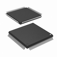
M30624FGNGP#D5 Renesas Electronics America, M30624FGNGP#D5 Datasheet - Page 159

M30624FGNGP#D5
Manufacturer Part Number
M30624FGNGP#D5
Description
IC M16C MCU FLASH 256K 100LQFP
Manufacturer
Renesas Electronics America
Series
M16C™ M16C/60r
Datasheet
1.M30620FCNGPU5.pdf
(250 pages)
Specifications of M30624FGNGP#D5
Core Processor
M16C/60
Core Size
16-Bit
Speed
16MHz
Connectivity
SIO, UART/USART
Peripherals
DMA, PWM, WDT
Number Of I /o
85
Program Memory Size
256KB (256K x 8)
Program Memory Type
FLASH
Ram Size
20K x 8
Voltage - Supply (vcc/vdd)
3 V ~ 3.6 V
Data Converters
A/D 18x10b, D/A 2x8b
Oscillator Type
Internal
Operating Temperature
-20°C ~ 85°C
Package / Case
100-LQFP
Lead Free Status / RoHS Status
Contains lead / RoHS non-compliant
Eeprom Size
-
Available stocks
Company
Part Number
Manufacturer
Quantity
Price
- Current page: 159 of 250
- Download datasheet (4Mb)
A-D Converter
156
Table 1.18.2. One-shot mode specifications
Note : AN
Figure 1.18.4. A-D conversion register in one-shot mode
(1) One-shot mode
Function
Start condition
Stop condition
Interrupt request generation timing End of A-D conversion
Input pin
Reading of result of A-D converter
In one-shot mode, the pin selected using the analog input pin select bit is used for one-shot A-D conver-
sion. Table 1.18.2 shows the specifications of one-shot mode. Figure 1.18.4 shows the A-D control regis-
ter in one-shot mode.
00
Item
to AN
A-D control register 0 (Note 1)
b7
A-D control register 1 (Note)
b7
07
b6
b6
can be used the same as AN
b5
b5
1
b4
b4
0
b3
0
b3
b2
b2
0
The pin selected by the analog input pin select bit is used for one A-D conversion
Writing “1” to A-D conversion start flag
• End of A-D conversion (A-D conversion start flag changes to “0”, except
• Writing “0” to A-D conversion start flag
One of AN
Read A-D register corresponding to selected pin
when external trigger is selected)
b1
b1
b0
b0
Note 1: If the A-D control register is rewritten during A-D conversion, the conversion
Note 2: AN
Note 3: When changing A-D operation mode, set analog input pin again.
Note: If the A-D control register is rewritten during A-D conversion, the conversion
Bit symbol
Bit symbol
SCAN0
SCAN1
ADST
CKS0
VCUT
MD0
MD1
TRG
CKS1
OPA0
OPA1
CH0
CH1
CH2
BITS
MD2
Symbol
ADCON0
Symbol
ADCON1
result is indeterminate.
0
result is indeterminate.
to AN
00
to AN
Analog input pin select
bit
Trigger select bit
A-D conversion start flag 0 : A-D conversion disabled
A-D operation mode
select bit 1
Vref connect bit
External op-amp
connection mode bit
A-D operation mode
select bit 0
Frequency select bit 0
A-D sweep pin
select bit
8/10-bit mode select bit
Frequency select bit1
7
, as selected (Note)
07
Bit name
Bit name
can be used the same as AN
0
to AN
Address
Address
03D6
03D7
16
16
7
Specification
.
Invalid in one-shot mode
Set to “0” when this mode is selected
0 : 8-bit mode
1 : 10-bit mode
0 : f
1 : f
1 : Vref connected
b7 b6
0 0 : ANEX0 and ANEX1 are not used
0 1 : ANEX0 input is A-D converted
1 0 : ANEX1 input is A-D converted
1 1 : External op-amp connection mode
0 0 : One-shot mode
1 : A-D conversion started
00000XXX
b2 b1 b0
0 0 0 : AN
0 0 1 : AN
0 1 0 : AN
0 1 1 : AN
1 0 0 : AN
1 0 1 : AN
1 1 0 : AN
1 1 1 : AN
b4 b3
0 : Software trigger
1 : AD
0: f
1: f
When reset
When reset
AD
AD
AD
AD
00
/4 is selected
/2 is selected
/2 or f
is selected
TRG
16
SINGLE-CHIP 16-BIT CMOS MICROCOMPUTER
0
1
2
3
4
5
6
7
trigger
AD
is selected
is selected
is selected
is selected
is selected
is selected
is selected
is selected
2
0
/4 is selected
to AN
Function
Function
7
.
(Note 2)
(Note 3)
(Note 3)
M16C / 62N Group
Mitsubishi microcomputers
R
R
W
W
Related parts for M30624FGNGP#D5
Image
Part Number
Description
Manufacturer
Datasheet
Request
R

Part Number:
Description:
KIT STARTER FOR M16C/29
Manufacturer:
Renesas Electronics America
Datasheet:

Part Number:
Description:
KIT STARTER FOR R8C/2D
Manufacturer:
Renesas Electronics America
Datasheet:

Part Number:
Description:
R0K33062P STARTER KIT
Manufacturer:
Renesas Electronics America
Datasheet:

Part Number:
Description:
KIT STARTER FOR R8C/23 E8A
Manufacturer:
Renesas Electronics America
Datasheet:

Part Number:
Description:
KIT STARTER FOR R8C/25
Manufacturer:
Renesas Electronics America
Datasheet:

Part Number:
Description:
KIT STARTER H8S2456 SHARPE DSPLY
Manufacturer:
Renesas Electronics America
Datasheet:

Part Number:
Description:
KIT STARTER FOR R8C38C
Manufacturer:
Renesas Electronics America
Datasheet:

Part Number:
Description:
KIT STARTER FOR R8C35C
Manufacturer:
Renesas Electronics America
Datasheet:

Part Number:
Description:
KIT STARTER FOR R8CL3AC+LCD APPS
Manufacturer:
Renesas Electronics America
Datasheet:

Part Number:
Description:
KIT STARTER FOR RX610
Manufacturer:
Renesas Electronics America
Datasheet:

Part Number:
Description:
KIT STARTER FOR R32C/118
Manufacturer:
Renesas Electronics America
Datasheet:

Part Number:
Description:
KIT DEV RSK-R8C/26-29
Manufacturer:
Renesas Electronics America
Datasheet:

Part Number:
Description:
KIT STARTER FOR SH7124
Manufacturer:
Renesas Electronics America
Datasheet:

Part Number:
Description:
KIT STARTER FOR H8SX/1622
Manufacturer:
Renesas Electronics America
Datasheet:

Part Number:
Description:
KIT DEV FOR SH7203
Manufacturer:
Renesas Electronics America
Datasheet:


