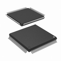
M30624FGNGP#D5 Renesas Electronics America, M30624FGNGP#D5 Datasheet - Page 123
M30624FGNGP#D5
Manufacturer Part Number
M30624FGNGP#D5
Description
IC M16C MCU FLASH 256K 100LQFP
Manufacturer
Renesas Electronics America
Series
M16C™ M16C/60r
Datasheet
1.M30620FCNGPU5.pdf
(250 pages)
Specifications of M30624FGNGP#D5
Core Processor
M16C/60
Core Size
16-Bit
Speed
16MHz
Connectivity
SIO, UART/USART
Peripherals
DMA, PWM, WDT
Number Of I /o
85
Program Memory Size
256KB (256K x 8)
Program Memory Type
FLASH
Ram Size
20K x 8
Voltage - Supply (vcc/vdd)
3 V ~ 3.6 V
Data Converters
A/D 18x10b, D/A 2x8b
Oscillator Type
Internal
Operating Temperature
-20°C ~ 85°C
Package / Case
100-LQFP
Lead Free Status / RoHS Status
Contains lead / RoHS non-compliant
Eeprom Size
-
Available stocks
Company
Part Number
Manufacturer
Quantity
Price


Serial I/O
120
Figure 1.17.9. Serial I/O-related registers (6)
UART2 special mode register 2 (I C bus exclusive use register)
UART2 special mode register 3 (I C bus exclusive use register)
b7 b6 b5 b4 b3 b2 b1 b0
b7 b6 b5 b4 b3 b2 b1 b0
Note 1: This bit can be read or written to when UART2 special mode register (U2SMR at address 0377
Note 2: These bits are initialized to “000” when SDDS = “0”. After a reset, these bits are set to “000”. However,
Note 3: The amount of delay varies with the load on SCL and SDA pins. Also, when using an external clock, the
7 (SDDS: SDA digital delay select bit) = “1”. When the initial value of UART2 special mode register 3
(U2SMR3) is read after setting SDDS = “1”, the value is “00
register 3 (U2SMR3) after setting SDDS = “1”, be sure to write 0's to bits 0–4. When SDDS = “0”,
this register cannot be written to; when read, the value is indeterminate.
because these bits can be read only when SDDS = “1”, the value read from these bits when SDDS = “0”
is indeterminate.
amount of delay increases by about 200 ns, so be sure to take this into account when using the device.
IICM2
CSC
ALS
STAC
SDHI
DL0
DL1
DL2
SWC
SWC2
SHTC
Nothing is assigned.
In an attempt to write to these bits, write “0”. The value, if read, turns out to be
indeterminate. However, when SDDS = “1”, the value “0” is read out (Note 1)
symbol
symbol
Bit
Bit
Symbol
Symbol
U2SMR2
U2SMR3
SDA output disable bit
Start/stop condition
control bit
I C mode select bit 2
Clock-synchronous bit
UART2 initialization bit
SDA digital delay setup
bit
(Note 1, Note 2, Note 3)
SCL wait output bit
SDA output stop bit
SCL wait output bit 2
2
2
2
Bit name
Bit name
Address
Address
0376
0375
16
16
b7 b6 b5
Refer to Table 1.17.11
0 : Disabled
1 : Enabled
0 : Disabled
1 : Enabled
0: UART2 clock
1: 0 output
0: Enabled
1: Disabled (high impedance)
0 0 0 : Must not be set when using I
0 0 1 : 1 to 2 cycle(s) of 1/f(X
0 1 0 : 2 to 3 cycles of 1/f(X
0 1 1 : 3 to 4 cycles of 1/f(X
1 0 0 : 4 to 5 cycles of 1/f(X
1 0 1 : 5 to 6 cycles of 1/f(X
1 1 0 : 6 to 7 cycles of 1/f(X
1 1 1 : 7 to 8 cycles of 1/f(X
0 : Disabled
1 : Enabled
0 : Disabled
1 : Enabled
Set this bit to “1” in I
(refer to Table 1.17.12)
When reset
When reset
(I C bus exclusive use register)
00
00
16
2
16
16
”. When writing to UART2 special mode
SINGLE-CHIP 16-BIT CMOS MICROCOMPUTER
(I
2
C bus exclusive use)
2
C mode
Function
Function
IN
IN
IN
IN
IN
IN
IN
)
)
)
)
)
)
)
2
C mode
Digital delay
is selected
M16C / 62N Group
Mitsubishi microcomputers
16
) bit
R
R
W
W
Related parts for M30624FGNGP#D5
Image
Part Number
Description
Manufacturer
Datasheet
Request
R

Part Number:
Description:
KIT STARTER FOR M16C/29
Manufacturer:
Renesas Electronics America
Datasheet:

Part Number:
Description:
KIT STARTER FOR R8C/2D
Manufacturer:
Renesas Electronics America
Datasheet:

Part Number:
Description:
R0K33062P STARTER KIT
Manufacturer:
Renesas Electronics America
Datasheet:

Part Number:
Description:
KIT STARTER FOR R8C/23 E8A
Manufacturer:
Renesas Electronics America
Datasheet:

Part Number:
Description:
KIT STARTER FOR R8C/25
Manufacturer:
Renesas Electronics America
Datasheet:

Part Number:
Description:
KIT STARTER H8S2456 SHARPE DSPLY
Manufacturer:
Renesas Electronics America
Datasheet:

Part Number:
Description:
KIT STARTER FOR R8C38C
Manufacturer:
Renesas Electronics America
Datasheet:

Part Number:
Description:
KIT STARTER FOR R8C35C
Manufacturer:
Renesas Electronics America
Datasheet:

Part Number:
Description:
KIT STARTER FOR R8CL3AC+LCD APPS
Manufacturer:
Renesas Electronics America
Datasheet:
Part Number:
Description:
KIT STARTER FOR RX610
Manufacturer:
Renesas Electronics America
Datasheet:

Part Number:
Description:
KIT STARTER FOR R32C/118
Manufacturer:
Renesas Electronics America
Datasheet:

Part Number:
Description:
KIT DEV RSK-R8C/26-29
Manufacturer:
Renesas Electronics America
Datasheet:

Part Number:
Description:
KIT STARTER FOR SH7124
Manufacturer:
Renesas Electronics America
Datasheet:

Part Number:
Description:
KIT STARTER FOR H8SX/1622
Manufacturer:
Renesas Electronics America
Datasheet:

Part Number:
Description:
KIT DEV FOR SH7203
Manufacturer:
Renesas Electronics America
Datasheet: