M30624FGNGP#D5 Renesas Electronics America, M30624FGNGP#D5 Datasheet - Page 26
M30624FGNGP#D5
Manufacturer Part Number
M30624FGNGP#D5
Description
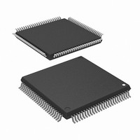
IC M16C MCU FLASH 256K 100LQFP
Manufacturer
Renesas Electronics America
Series
M16C™ M16C/60r
Datasheet
1.M30620FCNGPU5.pdf
(250 pages)
Specifications of M30624FGNGP#D5
Core Processor
M16C/60
Core Size
16-Bit
Speed
16MHz
Connectivity
SIO, UART/USART
Peripherals
DMA, PWM, WDT
Number Of I /o
85
Program Memory Size
256KB (256K x 8)
Program Memory Type
FLASH
Ram Size
20K x 8
Voltage - Supply (vcc/vdd)
3 V ~ 3.6 V
Data Converters
A/D 18x10b, D/A 2x8b
Oscillator Type
Internal
Operating Temperature
-20°C ~ 85°C
Package / Case
100-LQFP
Lead Free Status / RoHS Status
Contains lead / RoHS non-compliant
Eeprom Size
-
Available stocks
Company
Part Number
Manufacturer
Quantity
Price


Memory Space Expansion Features
The data bank register is made up of the bank selection bits (bits 5 through 3) and the offset bit (bit 2). The
bank selection bits are used to set a bank number for accessing data lying between 40000
BFFFF
Figure 1.7.3 shows the memory location and chip select areas in expansion mode.
The area relevant to CS0 ranges from 40000
BFFFF
- CS1 only in accessing data. In fetching a program, bank 7 (111
area from C0000
data or to fetching a program.
In accessing an area irrelevant to CS0, a chip select signal CS3 (4000
27FFF
Figure 1.7.4 shows an example of connecting the MCU with a 4-M byte ROM and to a 128-K byte SRAM.
Connect the chip select of 4-M byte ROM with CS0. Connect M16C’s CS3, CS2, and CS1 with address
inputs AD21, AD20, and AD19 respectively. Connect M16C’s output A19 with address input AD18. Fig-
ure 1.7.5 shows the relationship between addresses of the 4-M byte ROM and those of M16C.
In this mode, memory is
banked every 512 K bytes,
so that data access in differ-
ent banks requires switching
over banks. However, data
on bank boundaries when
offset bit = 0 can be ac-
cessed successively by set-
ting the offset bit to 1, be-
cause in which case the
memory address is offset by
40000
bytes of data located at ad-
d r e s s e s 0 F F F F F
100000
can be accessed succes-
sively without having to
change the bank bit by set-
ting the offset bit to 1 and
then accessing addresses
07FFFF
On the other hand, the
SRAM’s chip select assumes
that CS0=1 (not selected)
and CS2=0 (selected), so
connect CS0 with S2 and
_______
CS2 with S1. If the SRAM
doesn’t have a bipolar chip
select input terminal, decode
_______
CS0 and CS2 externally.
_______
_______
_______
16
16
16
16
16
16
), and CS1 (28000
. For example, two
. Assigning 1 to the offset bit provides the means to set offsets covering 40000
, the bank number set by use of the bank selection bits are output from the output terminals CS3
_______
_______
and 800000
of 4-Mbyte ROM
____
_______
16
through FFFFF
_______
1 6
16
a n d
.
16
- 3FFFF
Figure 1.7.4. An example of connecting the MCU with external
16
, bank 7 (111
_______
Note: If only one chip select terminal (S1 or S2) is present,
16
An example of connecting the MCU with
external memories in expansion mode
(M30620MCN, Microprocessor mode)
) is output depending on the address as in the past.
A0 to A16
decoding by use of an external circuit is required.
D0 to D7
16
CS1
CS2
CS3
CS0
_______
A17
A19
WR
RD
through FFFFF
memories in expansion mode
2
) is output from CS3 - CS1 without regard to accessing
17
8
SINGLE-CHIP 16-BIT CMOS MICROCOMPUTER
16
_______
. As for the area from 40000
2
_______
) is output from CS3 - CS1. As for the
_______
_______
DQ0 to DQ7
DQ0 to DQ7
OE
S2
AD0 to AD16
AD18
AD20
AD21
CS
AD0 to AD16
W
AD17
AD19
OE
S1
16
_______
- 7FFF
M16C / 62N Group
_______
Mitsubishi microcomputers
16
_______
), CS2 (8000
16
_______
_______
.
16
through
16
_______
and
16
-
23
Related parts for M30624FGNGP#D5
Image
Part Number
Description
Manufacturer
Datasheet
Request
R

Part Number:
Description:
KIT STARTER FOR M16C/29
Manufacturer:
Renesas Electronics America
Datasheet:

Part Number:
Description:
KIT STARTER FOR R8C/2D
Manufacturer:
Renesas Electronics America
Datasheet:

Part Number:
Description:
R0K33062P STARTER KIT
Manufacturer:
Renesas Electronics America
Datasheet:

Part Number:
Description:
KIT STARTER FOR R8C/23 E8A
Manufacturer:
Renesas Electronics America
Datasheet:

Part Number:
Description:
KIT STARTER FOR R8C/25
Manufacturer:
Renesas Electronics America
Datasheet:

Part Number:
Description:
KIT STARTER H8S2456 SHARPE DSPLY
Manufacturer:
Renesas Electronics America
Datasheet:

Part Number:
Description:
KIT STARTER FOR R8C38C
Manufacturer:
Renesas Electronics America
Datasheet:

Part Number:
Description:
KIT STARTER FOR R8C35C
Manufacturer:
Renesas Electronics America
Datasheet:

Part Number:
Description:
KIT STARTER FOR R8CL3AC+LCD APPS
Manufacturer:
Renesas Electronics America
Datasheet:
Part Number:
Description:
KIT STARTER FOR RX610
Manufacturer:
Renesas Electronics America
Datasheet:

Part Number:
Description:
KIT STARTER FOR R32C/118
Manufacturer:
Renesas Electronics America
Datasheet:

Part Number:
Description:
KIT DEV RSK-R8C/26-29
Manufacturer:
Renesas Electronics America
Datasheet:

Part Number:
Description:
KIT STARTER FOR SH7124
Manufacturer:
Renesas Electronics America
Datasheet:

Part Number:
Description:
KIT STARTER FOR H8SX/1622
Manufacturer:
Renesas Electronics America
Datasheet:

Part Number:
Description:
KIT DEV FOR SH7203
Manufacturer:
Renesas Electronics America
Datasheet: