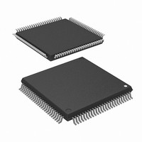
M30624FGNGP#D5 Renesas Electronics America, M30624FGNGP#D5 Datasheet - Page 198

M30624FGNGP#D5
Manufacturer Part Number
M30624FGNGP#D5
Description
IC M16C MCU FLASH 256K 100LQFP
Manufacturer
Renesas Electronics America
Series
M16C™ M16C/60r
Datasheet
1.M30620FCNGPU5.pdf
(250 pages)
Specifications of M30624FGNGP#D5
Core Processor
M16C/60
Core Size
16-Bit
Speed
16MHz
Connectivity
SIO, UART/USART
Peripherals
DMA, PWM, WDT
Number Of I /o
85
Program Memory Size
256KB (256K x 8)
Program Memory Type
FLASH
Ram Size
20K x 8
Voltage - Supply (vcc/vdd)
3 V ~ 3.6 V
Data Converters
A/D 18x10b, D/A 2x8b
Oscillator Type
Internal
Operating Temperature
-20°C ~ 85°C
Package / Case
100-LQFP
Lead Free Status / RoHS Status
Contains lead / RoHS non-compliant
Eeprom Size
-
Available stocks
Company
Part Number
Manufacturer
Quantity
Price
- Current page: 198 of 250
- Download datasheet (4Mb)
CPU Rewrite Mode (Flash Memory Version)
Figure 1.29.1. Flash identification register and flash memory control register 0
Bit 5 of the flash memory control register 0 is a user ROM area select bit which is effective in only boot
mode. If this bit is set to “1” in boot mode, the area to be accessed is switched from the boot ROM area to
the user ROM area. When the CPU rewrite mode needs to be used in boot mode, set this bit to “1”. Note
that if the microcomputer is booted from the user ROM area, it is always the user ROM area that can be
accessed and this bit has no effect. When in boot mode, the function of this bit is effective regardless of
whether the CPU rewrite mode is on or off. Write to this bit only when executing out of an area other than
the internal flash memory.
Bit 6 of the flash memory control register 0 is the program status flag used exclusively to read the operating
status of the auto program operation. If a program error occurs, it is set to “1”. Otherwise, it is “0”.
Bit 7 of the flash memory control register 0 is the erase status flag used exclusively to read the operating
status of the auto erase operation. If an erase error occurs, it is set to “1”. Otherwise, it is “0”.
Flash memory control register 0
b7 b6 b5 b4 b3 b2 b1 b0
Flash identification register
b7 b6 b5 b4 b3 b2 b1 b0
Note 1: For this bit to be set to “1”, the user needs to write a “0” and then a “1” to it in succession.
Note 2: For this bit to be set to “1”, the user needs to write a “0” and then a “1” to it in succession
Note 3: Effective only when the CPU rewrite mode select bit = 1. After write “1”, write “0” when
Note 4: Write to this bit only when executing out of an area other than the internal flash memory.
0
When it is not this procedure, it is not enacted in “1”. This is necessary to ensure that no
interrupt or DMA transfer will be executed during the interval. Write to this bit only when
executing out of an area other than the internal flash memory. Also only when NMI pin is
“H” level. Clear this bit to “0” after read array command.
when the CPU rewrite mode select bit = “1”. When it is not this procedure, it is not
enacted in “1”. This is necessary to ensure that no interrupt or DMA transfer will be
executed during the interval.
RY/BY status flag is “1”.
Procedure
(1) Write FF
(2) Read address 03B4
Reserved bit
Bit symbol
Bit symbol
FMR00
FMR01
FMR02
FMR03
FMR05
FMR06
FMR07
FIDR0
Symbol
Symbol
Read value = FF
Read value = 00
FMR0
FIDR
16
RY/BY status flag
CPU rewrite mode
select bit (Note 1)
Lock bit disable
select bit (Note 2)
User ROM area select bit
(Note 4) (Effective in only
boot mode)
Program status flag
Erase status flag
Flash memory reset bit
(Note 3)
Flash identification value
to the address 03B4
Bit name
Bit name
16
Address
Address
16 •••
03B7
03B4
16 •••
16
16
HND flash memory
DINOR flash memory
16
0: Busy (being written or erased)
1: Ready
0: Normal mode
1: CPU rewrite mode
0: Block lock by lock bit data is
1: Block lock by lock bit data is
0: Normal operation
1: Reset
Must always be set to “0”
0: Boot ROM area is accessed
1: User ROM area is accessed
0: Pass
1: Error
0: Pass
1: Error
Flash value output
HND:
When reset
When reset
(Software commands invalid)
(Software commands acceptable)
XX000001
enabled
disabled
00
00
16
16
SINGLE-CHIP 16-BIT CMOS MICROCOMPUTER
2
Function
Function
R
R
R W
R W
W
M16C / 62N Group
W
Mitsubishi microcomputers
195
Related parts for M30624FGNGP#D5
Image
Part Number
Description
Manufacturer
Datasheet
Request
R

Part Number:
Description:
KIT STARTER FOR M16C/29
Manufacturer:
Renesas Electronics America
Datasheet:

Part Number:
Description:
KIT STARTER FOR R8C/2D
Manufacturer:
Renesas Electronics America
Datasheet:

Part Number:
Description:
R0K33062P STARTER KIT
Manufacturer:
Renesas Electronics America
Datasheet:

Part Number:
Description:
KIT STARTER FOR R8C/23 E8A
Manufacturer:
Renesas Electronics America
Datasheet:

Part Number:
Description:
KIT STARTER FOR R8C/25
Manufacturer:
Renesas Electronics America
Datasheet:

Part Number:
Description:
KIT STARTER H8S2456 SHARPE DSPLY
Manufacturer:
Renesas Electronics America
Datasheet:

Part Number:
Description:
KIT STARTER FOR R8C38C
Manufacturer:
Renesas Electronics America
Datasheet:

Part Number:
Description:
KIT STARTER FOR R8C35C
Manufacturer:
Renesas Electronics America
Datasheet:

Part Number:
Description:
KIT STARTER FOR R8CL3AC+LCD APPS
Manufacturer:
Renesas Electronics America
Datasheet:

Part Number:
Description:
KIT STARTER FOR RX610
Manufacturer:
Renesas Electronics America
Datasheet:

Part Number:
Description:
KIT STARTER FOR R32C/118
Manufacturer:
Renesas Electronics America
Datasheet:

Part Number:
Description:
KIT DEV RSK-R8C/26-29
Manufacturer:
Renesas Electronics America
Datasheet:

Part Number:
Description:
KIT STARTER FOR SH7124
Manufacturer:
Renesas Electronics America
Datasheet:

Part Number:
Description:
KIT STARTER FOR H8SX/1622
Manufacturer:
Renesas Electronics America
Datasheet:

Part Number:
Description:
KIT DEV FOR SH7203
Manufacturer:
Renesas Electronics America
Datasheet:


