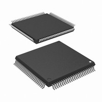
M30624FGNGP#D5 Renesas Electronics America, M30624FGNGP#D5 Datasheet - Page 201

M30624FGNGP#D5
Manufacturer Part Number
M30624FGNGP#D5
Description
IC M16C MCU FLASH 256K 100LQFP
Manufacturer
Renesas Electronics America
Series
M16C™ M16C/60r
Datasheet
1.M30620FCNGPU5.pdf
(250 pages)
Specifications of M30624FGNGP#D5
Core Processor
M16C/60
Core Size
16-Bit
Speed
16MHz
Connectivity
SIO, UART/USART
Peripherals
DMA, PWM, WDT
Number Of I /o
85
Program Memory Size
256KB (256K x 8)
Program Memory Type
FLASH
Ram Size
20K x 8
Voltage - Supply (vcc/vdd)
3 V ~ 3.6 V
Data Converters
A/D 18x10b, D/A 2x8b
Oscillator Type
Internal
Operating Temperature
-20°C ~ 85°C
Package / Case
100-LQFP
Lead Free Status / RoHS Status
Contains lead / RoHS non-compliant
Eeprom Size
-
Available stocks
Company
Part Number
Manufacturer
Quantity
Price
- Current page: 201 of 250
- Download datasheet (4Mb)
198
CPU Rewrite Mode (Flash Memory Version)
Table 1.29.1. List of software commands (CPU rewrite mode)
Note 1: When a software command is input, the high-order byte of data (D
Note 2: SRD = Status Register Data (Set an address to even address in the user ROM area)
Note 3: WA = Write Address (even address), WD = Write Data (16-bit data)
Note 4: BA = Block Address (Enter the maximum address of each block that is an even address.)
Note 5: D
Note 6: X denotes a given address in the user ROM area (that is an even address).
Software Commands
Read array
Read status register
Clear status register
Block erase
Lock bit program
Read lock bit status
Erase all unlock block
Program
Table 1.29.1 lists the software commands available with the M16C/62N (flash memory version).
After setting the CPU rewrite mode select bit to 1, write a software command to specify an erase or
program operation. Note that when entering a software command, the upper byte (D
The content of each software command is explained below.
Read Array Command (FF
Read Status Register Command (70
Clear Status Register Command (50
The read array mode is entered by writing the command code “FF
even address to be read is input in one of the bus cycles that follow, the content of the specified
address is read out at the data bus (D
The read array mode is retained intact until another command is written.
However, please begin to read data in the following procedures when a user uses read array com-
mand after program command.
(1) Set FF
(2) Input the top address which FF
(3) Input the top address till FFFF
(4) Input top address +2
(5) Input top address +2 till FFFF
(6) Input an arbitrary address
When the command code “70
read out at the data bus (D
in the user ROM area).
The status register is explained in the next section.
This command is used to clear the bits SR4 and SR5 of the status register after they have been set.
These bits indicate that operation has ended in an error. To use this command, write the command
code “50
Command
6
corresponds to the block lock status. Block not locked when D
16
16
” in the first bus cycle.
, FF
(Note 3)
16
, FF
16
, FF
Write
Write
Write
Write
Write
Write
Write
Write
16
Mode
0
–D
)
16
16
7
to arbitrary continuing four address beforehand
) by a read in the second bus cycle (Set an address to even address
” is written in the first bus cycle, the content of the status register is
16
16
16
First bus cycle
agrees with the value that begins to have been read
agrees with the value that begins to have been read
16
16
was set at (in read array mode)
Address
0
)
)
–D
WA
BA
X
X
X
X
X
X
15
), 16 bits at a time.
(D
0
Data
FF
A7
70
50
40
20
77
71
to D
16
16
16
16
16
16
16
16
7
)
SINGLE-CHIP 16-BIT CMOS MICROCOMPUTER
6
Mode
Read
Read
Write
Write
Write
Write
8
= 1, block locked when D
to D
16
” in the first bus cycle. When an
15
) is ignored.
Second bus cycle
WA
BA
Address
M16C / 62N Group
BA
BA
8
X
X
(Note 3)
Mitsubishi microcomputers
(Note 4)
to D
15
) is ignored.
SRD
D0
D0
D0
WD
(D
6
D
= 0.
16
16
16
6 (Note 5)
Data
0
to D
(Note 2)
(Note 3)
7
)
Related parts for M30624FGNGP#D5
Image
Part Number
Description
Manufacturer
Datasheet
Request
R

Part Number:
Description:
KIT STARTER FOR M16C/29
Manufacturer:
Renesas Electronics America
Datasheet:

Part Number:
Description:
KIT STARTER FOR R8C/2D
Manufacturer:
Renesas Electronics America
Datasheet:

Part Number:
Description:
R0K33062P STARTER KIT
Manufacturer:
Renesas Electronics America
Datasheet:

Part Number:
Description:
KIT STARTER FOR R8C/23 E8A
Manufacturer:
Renesas Electronics America
Datasheet:

Part Number:
Description:
KIT STARTER FOR R8C/25
Manufacturer:
Renesas Electronics America
Datasheet:

Part Number:
Description:
KIT STARTER H8S2456 SHARPE DSPLY
Manufacturer:
Renesas Electronics America
Datasheet:

Part Number:
Description:
KIT STARTER FOR R8C38C
Manufacturer:
Renesas Electronics America
Datasheet:

Part Number:
Description:
KIT STARTER FOR R8C35C
Manufacturer:
Renesas Electronics America
Datasheet:

Part Number:
Description:
KIT STARTER FOR R8CL3AC+LCD APPS
Manufacturer:
Renesas Electronics America
Datasheet:

Part Number:
Description:
KIT STARTER FOR RX610
Manufacturer:
Renesas Electronics America
Datasheet:

Part Number:
Description:
KIT STARTER FOR R32C/118
Manufacturer:
Renesas Electronics America
Datasheet:

Part Number:
Description:
KIT DEV RSK-R8C/26-29
Manufacturer:
Renesas Electronics America
Datasheet:

Part Number:
Description:
KIT STARTER FOR SH7124
Manufacturer:
Renesas Electronics America
Datasheet:

Part Number:
Description:
KIT STARTER FOR H8SX/1622
Manufacturer:
Renesas Electronics America
Datasheet:

Part Number:
Description:
KIT DEV FOR SH7203
Manufacturer:
Renesas Electronics America
Datasheet:


