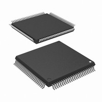
M30624FGNGP#D5 Renesas Electronics America, M30624FGNGP#D5 Datasheet - Page 163

M30624FGNGP#D5
Manufacturer Part Number
M30624FGNGP#D5
Description
IC M16C MCU FLASH 256K 100LQFP
Manufacturer
Renesas Electronics America
Series
M16C™ M16C/60r
Datasheet
1.M30620FCNGPU5.pdf
(250 pages)
Specifications of M30624FGNGP#D5
Core Processor
M16C/60
Core Size
16-Bit
Speed
16MHz
Connectivity
SIO, UART/USART
Peripherals
DMA, PWM, WDT
Number Of I /o
85
Program Memory Size
256KB (256K x 8)
Program Memory Type
FLASH
Ram Size
20K x 8
Voltage - Supply (vcc/vdd)
3 V ~ 3.6 V
Data Converters
A/D 18x10b, D/A 2x8b
Oscillator Type
Internal
Operating Temperature
-20°C ~ 85°C
Package / Case
100-LQFP
Lead Free Status / RoHS Status
Contains lead / RoHS non-compliant
Eeprom Size
-
Available stocks
Company
Part Number
Manufacturer
Quantity
Price
- Current page: 163 of 250
- Download datasheet (4Mb)
A-D Converter
160
Table 1.18.6. Repeat sweep mode 1 specifications
Note : AN
Figure 1.18.8. A-D conversion register in repeat sweep mode 1
(5) Repeat sweep mode 1
Function
Start condition
Stop condition
Interrupt request generation timing
Input pin
Reading of result of A-D converter
In repeat sweep mode 1, all pins are used for A-D conversion with emphasis on the pin or pins selected
using the A-D sweep pin select bit. Table 1.18.6 shows the specifications of repeat sweep mode 1. Figure
1.18.8 shows the A-D control register in repeat sweep mode 1.
00
Item
to AN
A-D control register 0 (Note)
A-D control register 1 (Note 1)
b7
b7
b6
b6
b5
b5
1
07
b4
1 1
b4
can be used the same as AN
b3
b3
b2
b2
1
b1
b1
b0
b0
All pins perform repeat A-D conversion, with emphasis on the pin or pins
selected by the A-D sweep pin select bit
Example : AN
Writing “1” to A-D conversion start flag
Writing “0” to A-D conversion start flag
None generated
With emphasis on these pins ; AN
Read A-D register corresponding to selected pin (at any time)
Note: If the A-D control register is rewritten during A-D conversion, the conversion result
Note 1: If the A-D control register is rewritten during A-D conversion, the conversion result
Note 2: AN
Note 3: Neither ‘01’ nor ‘10’ can be selected with the external op-amp connection mode bit.
Bit symbol
Bit symbol
SCAN0
SCAN1
CKS1
VCUT
OPA0
OPA1
BITS
ADST
CKS0
MD2
MD0
MD1
TRG
CH0
CH1
CH2
Symbol
ADCON1
Symbol
ADCON0
is indeterminate.
is indeterminate.
00
to AN
Analog input pin
select bit
Frequency select bit 0
A-D operation mode
select bit 0
Trigger select bit
A-D conversion start flag
A-D operation mode
select bit 1
8/10-bit mode select bit
Frequency select bit 1
Vref connect bit
External op-amp
connection mode
bit (Note 3)
A-D sweep pin select bit
07
Bit name
0
Bit name
can be used the same as AN
selected
Address
Address
03D6
03D7
16
16
0
to AN
00000XXX
When reset
When reset
When repeat sweep mode 1 is selected
Set to “1” when this mode is selected
0 : 8-bit mode
1 : 10-bit mode
0 : f
1 : f
1 : Vref connected
b7 b6
0 0 : ANEX0 and ANEX1 are not used
0 1 : ANEX0 input is A-D converted
1 0 : ANEX1 input is A-D converted
1 1 : External op-amp connection mode
Invalid in repeat sweep mode 1
b4 b3
1 1 : Repeat sweep mode 1
0 : Software trigger
1 : AD
0 : A-D conversion disabled
1 : A-D conversion started
0 : f
1 : f
0 0 : AN
0 1 : AN
1 0 : AN
1 1 : AN
b1 b0
AN
00
AD
AD
AD
AD
16
/2 or f
/4 is selected
/2 is selected
TRG
is selected
7
Specification
0
.
0
0
0
0
AN
, AN
(1 pin)
to AN
to AN
trigger
2
AD
0
1
/4 is selected
0
to AN
0
(2 pins)
2
3
AN
(3 pins)
(4 pins)
to AN
(1 pin), AN
Function
Function
7
SINGLE-CHIP 16-BIT CMOS MICROCOMPUTER
1
.
2
AN
(3 pins), AN
0
0
(Note 2)
and AN
AN
2
R
R
0
W
W
1
to AN
M16C / 62N Group
(2 pins),
AN
Mitsubishi microcomputers
0
3
(4 pins) (Note)
AN
3
, etc
Related parts for M30624FGNGP#D5
Image
Part Number
Description
Manufacturer
Datasheet
Request
R

Part Number:
Description:
KIT STARTER FOR M16C/29
Manufacturer:
Renesas Electronics America
Datasheet:

Part Number:
Description:
KIT STARTER FOR R8C/2D
Manufacturer:
Renesas Electronics America
Datasheet:

Part Number:
Description:
R0K33062P STARTER KIT
Manufacturer:
Renesas Electronics America
Datasheet:

Part Number:
Description:
KIT STARTER FOR R8C/23 E8A
Manufacturer:
Renesas Electronics America
Datasheet:

Part Number:
Description:
KIT STARTER FOR R8C/25
Manufacturer:
Renesas Electronics America
Datasheet:

Part Number:
Description:
KIT STARTER H8S2456 SHARPE DSPLY
Manufacturer:
Renesas Electronics America
Datasheet:

Part Number:
Description:
KIT STARTER FOR R8C38C
Manufacturer:
Renesas Electronics America
Datasheet:

Part Number:
Description:
KIT STARTER FOR R8C35C
Manufacturer:
Renesas Electronics America
Datasheet:

Part Number:
Description:
KIT STARTER FOR R8CL3AC+LCD APPS
Manufacturer:
Renesas Electronics America
Datasheet:

Part Number:
Description:
KIT STARTER FOR RX610
Manufacturer:
Renesas Electronics America
Datasheet:

Part Number:
Description:
KIT STARTER FOR R32C/118
Manufacturer:
Renesas Electronics America
Datasheet:

Part Number:
Description:
KIT DEV RSK-R8C/26-29
Manufacturer:
Renesas Electronics America
Datasheet:

Part Number:
Description:
KIT STARTER FOR SH7124
Manufacturer:
Renesas Electronics America
Datasheet:

Part Number:
Description:
KIT STARTER FOR H8SX/1622
Manufacturer:
Renesas Electronics America
Datasheet:

Part Number:
Description:
KIT DEV FOR SH7203
Manufacturer:
Renesas Electronics America
Datasheet:


