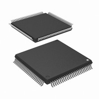
M30624FGNGP#D5 Renesas Electronics America, M30624FGNGP#D5 Datasheet - Page 215

M30624FGNGP#D5
Manufacturer Part Number
M30624FGNGP#D5
Description
IC M16C MCU FLASH 256K 100LQFP
Manufacturer
Renesas Electronics America
Series
M16C™ M16C/60r
Datasheet
1.M30620FCNGPU5.pdf
(250 pages)
Specifications of M30624FGNGP#D5
Core Processor
M16C/60
Core Size
16-Bit
Speed
16MHz
Connectivity
SIO, UART/USART
Peripherals
DMA, PWM, WDT
Number Of I /o
85
Program Memory Size
256KB (256K x 8)
Program Memory Type
FLASH
Ram Size
20K x 8
Voltage - Supply (vcc/vdd)
3 V ~ 3.6 V
Data Converters
A/D 18x10b, D/A 2x8b
Oscillator Type
Internal
Operating Temperature
-20°C ~ 85°C
Package / Case
100-LQFP
Lead Free Status / RoHS Status
Contains lead / RoHS non-compliant
Eeprom Size
-
Available stocks
Company
Part Number
Manufacturer
Quantity
Price
- Current page: 215 of 250
- Download datasheet (4Mb)
Mitsubishi microcomputers
M16C / 62N Group
Appendix Standard Serial I/O Mode (Flash Memory Version)
SINGLE-CHIP 16-BIT CMOS MICROCOMPUTER
Standard serial I/O mode
The standard serial I/O mode inputs and outputs the software commands, addresses and data needed to
operate (read, program, erase, etc.) the internal flash memory. This I/O is serial. There are actually two
standard serial I/O modes: mode 1, which is clock synchronized, and mode 2, which is asynchronized. Both
modes require a purpose-specific peripheral unit.
The standard serial I/O mode is different from the parallel I/O mode in that the CPU controls flash memory
rewrite (uses the CPU's rewrite mode), rewrite data input and so forth. It is started when the reset is re-
_____
________
leased, which is done when the P5
(CE) pin is "H" level, the P5
(EPM) pin "L" level and the CNVss pin "H"
0
5
level. (In the ordinary command mode, set CNVss pin to "L" level.)
This control program is written in the boot ROM area when the product is shipped from Mitsubishi. Accord-
ingly, make note of the fact that the standard serial I/O mode cannot be used if the boot ROM area is
rewritten in the parallel I/O mode. Figure 1.32.1 shows the pin connections for the standard serial I/O mode.
Serial data I/O uses UART1 and transfers the data serially in 8-bit units. Standard serial I/O switches
between mode 1 (clock synchronized) and mode 2 (clock asynchronized) according to the level of CLK
pin
1
when the reset is released.
To use standard serial I/O mode 1 (clock synchronized), set the CLK
pin to "H" level and release the reset.
1
The operation uses the four UART1 pins CLK
, RxD
, TxD
and RTS
(BUSY). The CLK
pin is the transfer
1
1
1
1
1
clock input pin through which an external transfer clock is input. The TxD
pin is for CMOS output. The
1
RTS
(BUSY) pin outputs an "L" level when ready for reception and an "H" level when reception starts.
1
To use standard serial I/O mode 2 (clock asynchronized), set the CLK
pin to "L" level and release the
1
reset. The operation uses the two UART1 pins RxD
and TxD
.
1
1
In the standard serial I/O mode, only the user ROM area indicated in Figure 1.32.18 can be rewritten. The
boot ROM cannot.
In the standard serial I/O mode, a 7-byte ID code is used. When there is data in the flash memory, com-
mands sent from the peripheral unit are not accepted unless the ID code matches.
212
Related parts for M30624FGNGP#D5
Image
Part Number
Description
Manufacturer
Datasheet
Request
R

Part Number:
Description:
KIT STARTER FOR M16C/29
Manufacturer:
Renesas Electronics America
Datasheet:

Part Number:
Description:
KIT STARTER FOR R8C/2D
Manufacturer:
Renesas Electronics America
Datasheet:

Part Number:
Description:
R0K33062P STARTER KIT
Manufacturer:
Renesas Electronics America
Datasheet:

Part Number:
Description:
KIT STARTER FOR R8C/23 E8A
Manufacturer:
Renesas Electronics America
Datasheet:

Part Number:
Description:
KIT STARTER FOR R8C/25
Manufacturer:
Renesas Electronics America
Datasheet:

Part Number:
Description:
KIT STARTER H8S2456 SHARPE DSPLY
Manufacturer:
Renesas Electronics America
Datasheet:

Part Number:
Description:
KIT STARTER FOR R8C38C
Manufacturer:
Renesas Electronics America
Datasheet:

Part Number:
Description:
KIT STARTER FOR R8C35C
Manufacturer:
Renesas Electronics America
Datasheet:

Part Number:
Description:
KIT STARTER FOR R8CL3AC+LCD APPS
Manufacturer:
Renesas Electronics America
Datasheet:

Part Number:
Description:
KIT STARTER FOR RX610
Manufacturer:
Renesas Electronics America
Datasheet:

Part Number:
Description:
KIT STARTER FOR R32C/118
Manufacturer:
Renesas Electronics America
Datasheet:

Part Number:
Description:
KIT DEV RSK-R8C/26-29
Manufacturer:
Renesas Electronics America
Datasheet:

Part Number:
Description:
KIT STARTER FOR SH7124
Manufacturer:
Renesas Electronics America
Datasheet:

Part Number:
Description:
KIT STARTER FOR H8SX/1622
Manufacturer:
Renesas Electronics America
Datasheet:

Part Number:
Description:
KIT DEV FOR SH7203
Manufacturer:
Renesas Electronics America
Datasheet:


