M30624FGNGP#D5 Renesas Electronics America, M30624FGNGP#D5 Datasheet - Page 36
M30624FGNGP#D5
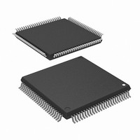
Manufacturer Part Number
M30624FGNGP#D5
Description
IC M16C MCU FLASH 256K 100LQFP
Manufacturer
Renesas Electronics America
Series
M16C™ M16C/60r
Datasheet
1.M30620FCNGPU5.pdf
(250 pages)
Specifications of M30624FGNGP#D5
Core Processor
M16C/60
Core Size
16-Bit
Speed
16MHz
Connectivity
SIO, UART/USART
Peripherals
DMA, PWM, WDT
Number Of I /o
85
Program Memory Size
256KB (256K x 8)
Program Memory Type
FLASH
Ram Size
20K x 8
Voltage - Supply (vcc/vdd)
3 V ~ 3.6 V
Data Converters
A/D 18x10b, D/A 2x8b
Oscillator Type
Internal
Operating Temperature
-20°C ~ 85°C
Package / Case
100-LQFP
Lead Free Status / RoHS Status
Contains lead / RoHS non-compliant
Eeprom Size
-
Available stocks
Company
Part Number
Manufacturer
Quantity
Price


Bus Control
Figure 1.10.2. Output Examples about Address Bus and Chip Select Signal (Separated Bus
Example 3) After access the external area, only the address bus changes
In this example, after access to the external area(i), an access to the area
indicated by the same chip select signal(i) will occur in the next cycle. In
this case, the address bus changes between the two cycles, but the chip
select signal does not change.
Example 1) After access the external area, both the address signal and
In this example, after access to the external area(i), an access to the area
indicated by the other chip select signal(j) will occur in the next cycle. In
this case, both the address bus and the chip select signal change between
the two cycles.
Address bus
Address bus
Read/Write
Chip select
Read/Write
Chip select
Chip select
Data bus
signal
(CS i)
Data bus
signal
(CS i)
(CS j)
BCLK
in the next cycle (the chip select signal does not change).
BCLK
the chip select signal change concurrently in the next cycle.
without Wait)
Note : These examples show the address bus and chip select signal within the successive two cycles.
Access to the
External Area( i )
Access to the
External Area( i )
According to the combination of these examples, the chip select can be elongated to over 2cycles.
Address
Address
Data
Data
Access to the Same
External Area( i )
Access to the Other
External Area( j )
Example 2) After access the external area, only the chip select signal
In this example, an access to the internal ROM or the internal RAM in the
next cycle will occur, after access to the external area. In this case, the
chip select signal changes between the two cycles, but the address does
not change.
Example 4) After access the external area, either the address signal and
In this example, any access to any area does not occur in the next cycle
(either instruction prefetch does not occur). In this case,either the address
bus and chip select signal do not change between the two cycles.
Address bus
Read/Write
Chip select
Address bus
Chip select
Read/Write
Data bus
signal
Data bus
signal
changes in the next cycle (the address bus does not change).
the chip select signal do not change in the next cycle.
BCLK
SINGLE-CHIP 16-BIT CMOS MICROCOMPUTER
BCLK
Access to the
External Area
Access to the
External Area
Address
Address
Data
Data
No Access
M16C / 62N Group
Internal ROM/RAM
Access
Mitsubishi microcomputers
33
Related parts for M30624FGNGP#D5
Image
Part Number
Description
Manufacturer
Datasheet
Request
R

Part Number:
Description:
KIT STARTER FOR M16C/29
Manufacturer:
Renesas Electronics America
Datasheet:

Part Number:
Description:
KIT STARTER FOR R8C/2D
Manufacturer:
Renesas Electronics America
Datasheet:

Part Number:
Description:
R0K33062P STARTER KIT
Manufacturer:
Renesas Electronics America
Datasheet:

Part Number:
Description:
KIT STARTER FOR R8C/23 E8A
Manufacturer:
Renesas Electronics America
Datasheet:

Part Number:
Description:
KIT STARTER FOR R8C/25
Manufacturer:
Renesas Electronics America
Datasheet:

Part Number:
Description:
KIT STARTER H8S2456 SHARPE DSPLY
Manufacturer:
Renesas Electronics America
Datasheet:

Part Number:
Description:
KIT STARTER FOR R8C38C
Manufacturer:
Renesas Electronics America
Datasheet:

Part Number:
Description:
KIT STARTER FOR R8C35C
Manufacturer:
Renesas Electronics America
Datasheet:

Part Number:
Description:
KIT STARTER FOR R8CL3AC+LCD APPS
Manufacturer:
Renesas Electronics America
Datasheet:
Part Number:
Description:
KIT STARTER FOR RX610
Manufacturer:
Renesas Electronics America
Datasheet:

Part Number:
Description:
KIT STARTER FOR R32C/118
Manufacturer:
Renesas Electronics America
Datasheet:

Part Number:
Description:
KIT DEV RSK-R8C/26-29
Manufacturer:
Renesas Electronics America
Datasheet:

Part Number:
Description:
KIT STARTER FOR SH7124
Manufacturer:
Renesas Electronics America
Datasheet:

Part Number:
Description:
KIT STARTER FOR H8SX/1622
Manufacturer:
Renesas Electronics America
Datasheet:

Part Number:
Description:
KIT DEV FOR SH7203
Manufacturer:
Renesas Electronics America
Datasheet: