M30624FGNGP#D5 Renesas Electronics America, M30624FGNGP#D5 Datasheet - Page 180
M30624FGNGP#D5
Manufacturer Part Number
M30624FGNGP#D5
Description
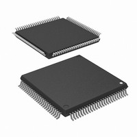
IC M16C MCU FLASH 256K 100LQFP
Manufacturer
Renesas Electronics America
Series
M16C™ M16C/60r
Datasheet
1.M30620FCNGPU5.pdf
(250 pages)
Specifications of M30624FGNGP#D5
Core Processor
M16C/60
Core Size
16-Bit
Speed
16MHz
Connectivity
SIO, UART/USART
Peripherals
DMA, PWM, WDT
Number Of I /o
85
Program Memory Size
256KB (256K x 8)
Program Memory Type
FLASH
Ram Size
20K x 8
Voltage - Supply (vcc/vdd)
3 V ~ 3.6 V
Data Converters
A/D 18x10b, D/A 2x8b
Oscillator Type
Internal
Operating Temperature
-20°C ~ 85°C
Package / Case
100-LQFP
Lead Free Status / RoHS Status
Contains lead / RoHS non-compliant
Eeprom Size
-
Available stocks
Company
Part Number
Manufacturer
Quantity
Price


Electrical characteristics
Table 1.26.2. Recommended operating conditions (referenced to V
Note 1: The mean output current is the mean value within 100ms.
Note 2: The total I
Note 3: Specify a product of -40 C to 85 C to use it.
Note 4: 2.2V is minimum supply voltage of mask ROM version.
Note 5: Relationship between main clock oscillation frequency and supply voltage.
Note 6: Execute case without wait, program / erase of flash memory by V
S y m b o l
f (X
f ( X c
Vcc
A V c c
V s s
A V s s
V
V
I
I
I
I
O H ( p e a k )
O H ( a v g )
O L ( p e a k )
OL (avg)
I H
I L
IN
I N
)
)
with wait, program / erase of flash memory by V
P2, P8
80mA max. The total I
Main clock input oscillation frequency (No wait)
16.0
Supply voltage
A n a l o g s u p p l y v o l t a g e
S u p p l y v o l t a g e
A n a l o g s u p p l y v o l t a g e
H I G H i n p u t
v o l t a g e
L O W i n p u t
v o l t a g e
HIGH average output
current
LOW average
output current
S u b c l o c k o s c i l l a t i o n f r e q u e n c y
H I G H p e a k o u t p u t
c u r r e n t
LOW peak output
current
7.0
3.5
0.0
Main clock input
oscillation
frequency
(Note 5, Note 6)
17.5 X V
6
, P8
Mask ROM version
Mask ROM and flash memory versions
15 X V
CC–
2.2
OL
3.6V at Topr = –20 C to 85
35MH
(BCLK: no division)
7
CC –
Supply voltage
(peak) for ports P0, P1, P2, P8
, P9, and P10 must be 80mA max. The total I
2.4
Z
29MH
Z
X
P 3
P 7
P 7
P 0
P 0
( d a t a i n p u t f u n c t i o n d u r i n g m e m o r y e x p a n s i o n a n d m i c r o p r o c e s s o r m o d e s )
P 3
P 7
X
P 0
P0
( d a t a i n p u t f u n c t i o n d u r i n g m e m o r y e x p a n s i o n a n d m i c r o p r o c e s s o r m o d e s )
3.0
I N
I N
[V]
1
2
0
0
0
1
0
0
0
, R E S E T , C N V
, R E S E T , C N V
,
t o P 3
t o P 7
t o P 0
t o P 0
t o P 3
t o P 7
t o P 0
to P0
P 7
OH
1
P0
P4
P8
P 0
P 4
P 8
No
wait
P0
P 4
P 8
P 0
P4
P8
With
wait
(peak) for ports P3, P4, P5, P6, P7
3.6
7
7
7
7
7
7
7
7
, P 4
, P 8
, P 1
, P 1
, P 4
, P 8
, P 1
, P1
0
0
0
0
0
0
0
0
0
0
0
0
t o P 0
t o P 4
t o P 8
to P0
to P4
to P8
to P0
t o P 4
t o P 8
t o P 0
to P4
to P8
0
0
0
0
0
0
0
0
t o P 4
t o P 8
t o P 1
t o P 1
t o P 4
t o P 8
t o P 1
to P1
7
7
4
7
7
4
S S
S S
7
7
4
7
7
4
, P 1
, P 5
, P 8
, P1
, P5
, P8
, P1
, P 5
, P 8
, P 1
, P5
, P8
Mask ROM version
Flash memory version
Mask ROM version
Mask ROM version
Flash memory version
Mask ROM version
, B Y T E
, B Y T E
P a r a m e t e r
7
7
7
7
7
7
7
7
, P 5
, P 9
, P 2
, P 2
, P 5
, P 9
, P 2
, P2
6
6
0
0
6
6
0
0
0
0
0
0
Main clock input oscillation frequency (With wait)
16.0
9.25
, P 8
, P8
, P 8
, P8
7.0
0.0
to P1
to P5
t o P 1
t o P 5
to P1
t o P 5
t o P 1
to P5
0
0
0
0
0
0
0
0
o
7
7
7
7
C / – 40 C to 85
t o P 5
t o P 9
t o P 2
t o P 2
t o P 5
t o P 9
t o P 2
to P2
11.25 X V
, P9
, P 9
, P 9
, P9
Mask ROM version
Mask ROM and flash memory versions
6
7
7
7
7
7
7
7
7
, P8
, P2
, P6
, P 2
, P 6
, P2
, P 6
, P 2
, P6
2.2
0
0
0
0
CC
7 ,
7
7
7
7 ,
7
7
7
to P9
t o P 9
CC
t o P 9
to P9
(BCLK: no division)
, P 1 0
, P 3
, P 3
, P 1 0
, P 3
, P3
–17.75MH
0
0
0
0
0
0
0
0
2.4
Supply voltage
P 6
P 6
7
t o P 2
t o P 6
to P2
to P6
to P2
t o P 6
t o P 2
to P6
, P9, and P10 must be 80mA max. The total I
=3.0V to 3.6V and f(BCLK)
0
0
0
0
0
0
7
7
Z
7
7
t o P 6
0
t o P 6
0
, P 1 0
( d u r i n g s i n g l e - c h i p m o d e )
( d u r i n g s i n g l e - c h i p m o d e )
, P10
, P 1 0
, P10
3.0
t o P 1 0
t o P 1 0
7
7
7
7
7
7
7
7
, P 3
, P 7
, P3
, P7
, P3
, P 7
, P 3
, P7
[V]
7
7
0
0
0
0
OL
,
,
0
2
0
2
0
0
0
0
t o P 1 0
to P10
t o P 1 0
to P10
7
7
2
to P3
to P7
t o P 3
t o P 7
to P3
t o P 7
t o P 3
to P7
o
3.6
,
,
(peak) for ports P3, P4, P5, P6, P7, and P8
Vcc=3.0V to 3.6V
Vcc=2.4V to 3.0V
V c c = 2 . 2 V t o 2 . 4 V
Vcc=3.0V to 3.6V
V c c = 2 . 4 V t o 3 . 0 V
V c c = 2 . 2 V t o 2 . 4 V
C(Note 3) unless otherwise specified)
to P7
CC
7
7
7
7
7
7
7
7
7
7
7
7
,
,
,
,
,
,
,
,
7
=3.0V to 3.6V and f(BCLK)
, and P8
SINGLE-CHIP 16-BIT CMOS MICROCOMPUTER
CC
Flash program/erase voltage
V
CC
=3.0V to 3.6V
0
= 2.4V (Mask ROM version is 2.2V) to
to P8
2.4 (Note 4)
10.0 MHz.
0 . 8 V c c
0 . 8 V c c
0.8Vcc
0 . 5 V c c
Flash memory version program/erase voltage and read
Min.
0
0
0
0
0
0
0
0
0
4
must be 80mA max.
operation voltage characteristics
S t a n d a r d
32.768
T y p .
V c c
3.3
0
0
OH
M16C / 62N Group
Mitsubishi microcomputers
6.25 MHz. Execute case
(peak) for ports P0, P1,
11.25 X Vcc
11.25 X Vcc
1 7 . 5 X V c c
Flash read operation voltage
V
1 5 X V c c
0 . 1 6 V c c
CC
0 . 2 V c c
0 . 2 V c c
- 17.75
- 17.75
0
M a x .
- 1 0 . 0
- 5 . 0
1 0 . 0
=2.4V to 3.6V
V c c
V c c
V c c
- 2 9
- 3 5
3.6
4.2
5 . 0
1 6
16
5 0
to P8
4
must be
U n i t
MHz
M H z
M H z
M H z
MHz
MHz
k H z
m A
m A
m A
m A
V
V
V
V
V
V
V
V
V
V
V
177
Related parts for M30624FGNGP#D5
Image
Part Number
Description
Manufacturer
Datasheet
Request
R

Part Number:
Description:
KIT STARTER FOR M16C/29
Manufacturer:
Renesas Electronics America
Datasheet:

Part Number:
Description:
KIT STARTER FOR R8C/2D
Manufacturer:
Renesas Electronics America
Datasheet:

Part Number:
Description:
R0K33062P STARTER KIT
Manufacturer:
Renesas Electronics America
Datasheet:

Part Number:
Description:
KIT STARTER FOR R8C/23 E8A
Manufacturer:
Renesas Electronics America
Datasheet:

Part Number:
Description:
KIT STARTER FOR R8C/25
Manufacturer:
Renesas Electronics America
Datasheet:

Part Number:
Description:
KIT STARTER H8S2456 SHARPE DSPLY
Manufacturer:
Renesas Electronics America
Datasheet:

Part Number:
Description:
KIT STARTER FOR R8C38C
Manufacturer:
Renesas Electronics America
Datasheet:

Part Number:
Description:
KIT STARTER FOR R8C35C
Manufacturer:
Renesas Electronics America
Datasheet:

Part Number:
Description:
KIT STARTER FOR R8CL3AC+LCD APPS
Manufacturer:
Renesas Electronics America
Datasheet:
Part Number:
Description:
KIT STARTER FOR RX610
Manufacturer:
Renesas Electronics America
Datasheet:

Part Number:
Description:
KIT STARTER FOR R32C/118
Manufacturer:
Renesas Electronics America
Datasheet:

Part Number:
Description:
KIT DEV RSK-R8C/26-29
Manufacturer:
Renesas Electronics America
Datasheet:

Part Number:
Description:
KIT STARTER FOR SH7124
Manufacturer:
Renesas Electronics America
Datasheet:

Part Number:
Description:
KIT STARTER FOR H8SX/1622
Manufacturer:
Renesas Electronics America
Datasheet:

Part Number:
Description:
KIT DEV FOR SH7203
Manufacturer:
Renesas Electronics America
Datasheet: