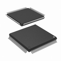
M30624FGNGP#D5 Renesas Electronics America, M30624FGNGP#D5 Datasheet - Page 196

M30624FGNGP#D5
Manufacturer Part Number
M30624FGNGP#D5
Description
IC M16C MCU FLASH 256K 100LQFP
Manufacturer
Renesas Electronics America
Series
M16C™ M16C/60r
Datasheet
1.M30620FCNGPU5.pdf
(250 pages)
Specifications of M30624FGNGP#D5
Core Processor
M16C/60
Core Size
16-Bit
Speed
16MHz
Connectivity
SIO, UART/USART
Peripherals
DMA, PWM, WDT
Number Of I /o
85
Program Memory Size
256KB (256K x 8)
Program Memory Type
FLASH
Ram Size
20K x 8
Voltage - Supply (vcc/vdd)
3 V ~ 3.6 V
Data Converters
A/D 18x10b, D/A 2x8b
Oscillator Type
Internal
Operating Temperature
-20°C ~ 85°C
Package / Case
100-LQFP
Lead Free Status / RoHS Status
Contains lead / RoHS non-compliant
Eeprom Size
-
Available stocks
Company
Part Number
Manufacturer
Quantity
Price
- Current page: 196 of 250
- Download datasheet (4Mb)
CPU Rewrite Mode (Flash Memory Version)
CPU Rewrite Mode
In CPU rewrite mode, the on-chip flash memory can be operated on (read, program, or erase) under control
of the Central Processing Unit (CPU).
In CPU rewrite mode, only the user ROM area shown in Figure 1.28.1 can be rewritten; the boot ROM area
cannot be rewritten. Make sure the program and block erase commands are issued for only the user ROM
area and each block area.
The control program for CPU rewrite mode can be stored in either user ROM or boot ROM area. In the CPU
rewrite mode, because the flash memory cannot be read from the CPU, the rewrite control program must
be transferred to any area other than the internal flash memory before it can be executed.
Microcomputer Mode and Boot Mode
Block Address
The control program for CPU rewrite mode must be written into the user ROM or boot ROM area in
parallel I/O mode beforehand. (If the control program is written into the boot ROM area, the standard
serial I/O mode becomes unusable.)
See Figure 1.28.1 for details about the boot ROM area.
Normal microcomputer mode is entered when the microcomputer is reset with pulling CNV
this case, the CPU starts operating using the control program in the user ROM area.
When the microcomputer is reset by pulling the P5
CPU starts operating using the control program in the boot ROM area. This mode is called the “boot”
mode. The control program in the boot ROM area can also be used to rewrite the user ROM area (When
rewriting the user ROM area in boot mode, bit 5 of the flash memory control register 0 must be set to “1”.
Write to this bit only when executing out of an area other than the internal flash memory).
Block addresses refer to an even address of each block. These addresses are used in the block erase
command, lock bit program command, and read lock status command.
5
pin low, the CNV
SINGLE-CHIP 16-BIT CMOS MICROCOMPUTER
SS
pin high, and the P5
M16C / 62N Group
Mitsubishi microcomputers
0
SS
pin high, the
pin low. In
193
Related parts for M30624FGNGP#D5
Image
Part Number
Description
Manufacturer
Datasheet
Request
R

Part Number:
Description:
KIT STARTER FOR M16C/29
Manufacturer:
Renesas Electronics America
Datasheet:

Part Number:
Description:
KIT STARTER FOR R8C/2D
Manufacturer:
Renesas Electronics America
Datasheet:

Part Number:
Description:
R0K33062P STARTER KIT
Manufacturer:
Renesas Electronics America
Datasheet:

Part Number:
Description:
KIT STARTER FOR R8C/23 E8A
Manufacturer:
Renesas Electronics America
Datasheet:

Part Number:
Description:
KIT STARTER FOR R8C/25
Manufacturer:
Renesas Electronics America
Datasheet:

Part Number:
Description:
KIT STARTER H8S2456 SHARPE DSPLY
Manufacturer:
Renesas Electronics America
Datasheet:

Part Number:
Description:
KIT STARTER FOR R8C38C
Manufacturer:
Renesas Electronics America
Datasheet:

Part Number:
Description:
KIT STARTER FOR R8C35C
Manufacturer:
Renesas Electronics America
Datasheet:

Part Number:
Description:
KIT STARTER FOR R8CL3AC+LCD APPS
Manufacturer:
Renesas Electronics America
Datasheet:

Part Number:
Description:
KIT STARTER FOR RX610
Manufacturer:
Renesas Electronics America
Datasheet:

Part Number:
Description:
KIT STARTER FOR R32C/118
Manufacturer:
Renesas Electronics America
Datasheet:

Part Number:
Description:
KIT DEV RSK-R8C/26-29
Manufacturer:
Renesas Electronics America
Datasheet:

Part Number:
Description:
KIT STARTER FOR SH7124
Manufacturer:
Renesas Electronics America
Datasheet:

Part Number:
Description:
KIT STARTER FOR H8SX/1622
Manufacturer:
Renesas Electronics America
Datasheet:

Part Number:
Description:
KIT DEV FOR SH7203
Manufacturer:
Renesas Electronics America
Datasheet:


