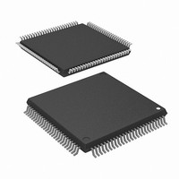
M30624FGNGP#D5 Renesas Electronics America, M30624FGNGP#D5 Datasheet - Page 217

M30624FGNGP#D5
Manufacturer Part Number
M30624FGNGP#D5
Description
IC M16C MCU FLASH 256K 100LQFP
Manufacturer
Renesas Electronics America
Series
M16C™ M16C/60r
Datasheet
1.M30620FCNGPU5.pdf
(250 pages)
Specifications of M30624FGNGP#D5
Core Processor
M16C/60
Core Size
16-Bit
Speed
16MHz
Connectivity
SIO, UART/USART
Peripherals
DMA, PWM, WDT
Number Of I /o
85
Program Memory Size
256KB (256K x 8)
Program Memory Type
FLASH
Ram Size
20K x 8
Voltage - Supply (vcc/vdd)
3 V ~ 3.6 V
Data Converters
A/D 18x10b, D/A 2x8b
Oscillator Type
Internal
Operating Temperature
-20°C ~ 85°C
Package / Case
100-LQFP
Lead Free Status / RoHS Status
Contains lead / RoHS non-compliant
Eeprom Size
-
Available stocks
Company
Part Number
Manufacturer
Quantity
Price
- Current page: 217 of 250
- Download datasheet (4Mb)
214
Appendix Standard Serial I/O Mode 1 (Flash Memory Version)
Note 1: Shading indicates transfer from flash memory microcomputer to peripheral unit. All other data is trans-
Note 2: SRD refers to status register data. SRD1 refers to status register 1 data.
Note 3: All commands can be accepted when the flash memory is totally blank.
10 Lock bit disable
11 ID check function
12 Download function
13 Version data output function
14 Boot ROM area output
15 Read check data
1
2
3
4
5
6
7
8
9
Table 1.32.1. Software commands (Standard serial I/O mode 1)
Software Commands
Page read
Page program
Block erase
Erase all unlocked blocks
Read status register
Clear status register
Read lock bit status
Lock bit program
Lock bit enable
function
Table 1.32.1 lists software commands. In the standard serial I/O mode 1, erase operations, programs and
reading are controlled by transferring software commands via the RxD
explained here below.
Control command
ferred from the peripheral unit to the flash memory microcomputer.
1st byte
transfer
FC
FD
FF
A7
7A
FA
FB
41
20
70
50
71
77
75
F5
16
16
16
16
16
16
16
16
16
16
16
16
16
16
16
Size (low)
data (low)
Address
(middle)
Address
(middle)
Address
(middle)
Address
(middle)
Address
(middle)
Address
Address
(middle)
Version
2nd byte
Check
output
output
(low)
D0
SRD
data
16
Address
Address
Address
Address
Address
Address
(middle)
Address
3rd byte
Version
output
output
Check
(high)
(high)
(high)
SRD1
(high)
(high)
(high)
(high)
(high)
Size
data
data
Address
Lock bit
Version
Check-
4th byte 5th byte 6th byte
output
output
output
output
(high)
Data
Data
input
D0
D0
Data
data
sum
data
16
16
SINGLE-CHIP 16-BIT CMOS MICROCOMPUTER
Version
ID size
output
output
output
Data
Data
input
Data
input
Data
data
1
pin. Software commands are
required
of times
Version
number
output
output
output
Data
Data
input
Data
data
ID1
To
M16C / 62N Group
259th byte
Data input
output to
output to
output to
to 259th
Mitsubishi microcomputers
9th byte
Version
To ID7
259th
Data
Data
byte
data
byte
When ID is
not verified
Acceptable
Acceptable
Acceptable
acceptable
acceptable
acceptable
acceptable
acceptable
acceptable
acceptable
acceptable
acceptable
acceptable
acceptable
acceptable
Not
Not
Not
Not
Not
Not
Not
Not
Not
Not
Not
Not
Related parts for M30624FGNGP#D5
Image
Part Number
Description
Manufacturer
Datasheet
Request
R

Part Number:
Description:
KIT STARTER FOR M16C/29
Manufacturer:
Renesas Electronics America
Datasheet:

Part Number:
Description:
KIT STARTER FOR R8C/2D
Manufacturer:
Renesas Electronics America
Datasheet:

Part Number:
Description:
R0K33062P STARTER KIT
Manufacturer:
Renesas Electronics America
Datasheet:

Part Number:
Description:
KIT STARTER FOR R8C/23 E8A
Manufacturer:
Renesas Electronics America
Datasheet:

Part Number:
Description:
KIT STARTER FOR R8C/25
Manufacturer:
Renesas Electronics America
Datasheet:

Part Number:
Description:
KIT STARTER H8S2456 SHARPE DSPLY
Manufacturer:
Renesas Electronics America
Datasheet:

Part Number:
Description:
KIT STARTER FOR R8C38C
Manufacturer:
Renesas Electronics America
Datasheet:

Part Number:
Description:
KIT STARTER FOR R8C35C
Manufacturer:
Renesas Electronics America
Datasheet:

Part Number:
Description:
KIT STARTER FOR R8CL3AC+LCD APPS
Manufacturer:
Renesas Electronics America
Datasheet:

Part Number:
Description:
KIT STARTER FOR RX610
Manufacturer:
Renesas Electronics America
Datasheet:

Part Number:
Description:
KIT STARTER FOR R32C/118
Manufacturer:
Renesas Electronics America
Datasheet:

Part Number:
Description:
KIT DEV RSK-R8C/26-29
Manufacturer:
Renesas Electronics America
Datasheet:

Part Number:
Description:
KIT STARTER FOR SH7124
Manufacturer:
Renesas Electronics America
Datasheet:

Part Number:
Description:
KIT STARTER FOR H8SX/1622
Manufacturer:
Renesas Electronics America
Datasheet:

Part Number:
Description:
KIT DEV FOR SH7203
Manufacturer:
Renesas Electronics America
Datasheet:


