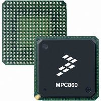
MC68EN360ZQ25VL Freescale Semiconductor, MC68EN360ZQ25VL Datasheet - Page 144

MC68EN360ZQ25VL
Manufacturer Part Number
MC68EN360ZQ25VL
Description
IC MPU QUICC 32BIT 357-PBGA
Manufacturer
Freescale Semiconductor
Datasheets
1.MC68EN302AG20BT.pdf
(8 pages)
2.MC68EN360VR25L.pdf
(14 pages)
3.MC68EN360VR25L.pdf
(2 pages)
4.MC68EN360ZQ25VL.pdf
(962 pages)
Specifications of MC68EN360ZQ25VL
Processor Type
M683xx 32-Bit
Speed
25MHz
Voltage
3.3V
Mounting Type
Surface Mount
Package / Case
357-PBGA
Family Name
M68xxx
Device Core
ColdFire
Device Core Size
32b
Frequency (max)
25MHz
Instruction Set Architecture
RISC
Supply Voltage 1 (typ)
3V
Operating Supply Voltage (max)
3.3V
Operating Supply Voltage (min)
2.7V
Operating Temp Range
0C to 70C
Operating Temperature Classification
Commercial
Mounting
Surface Mount
Pin Count
357
Package Type
BGA
Lead Free Status / RoHS Status
Contains lead / RoHS non-compliant
Features
-
Lead Free Status / Rohs Status
Not Compliant
Available stocks
Company
Part Number
Manufacturer
Quantity
Price
Company:
Part Number:
MC68EN360ZQ25VL
Manufacturer:
Freescale Semiconductor
Quantity:
10 000
- MC68EN302AG20BT PDF datasheet
- MC68EN360VR25L PDF datasheet #2
- MC68EN360VR25L PDF datasheet #3
- MC68EN360ZQ25VL PDF datasheet #4
- Current page: 144 of 962
- Download datasheet (4Mb)
CPU32+
aligned on their natural boundaries. All instruction words and extension words must reside
on word boundaries. Attempting to prefetch an instruction word at an odd address causes
an address error exception.
The CPU32+ has four bits (SZ1, SZ0 and SZC1, SCZ0) in the software status word (SSW)
that are new or have changed definitions.
The CPU32+ offers low power consumption. The CPU32+ is implemented in high-speed
complementary metal-oxide semiconductor (HCMOS) technology, providing low power use
during normal operation. During periods of inactivity, the low-power stop (LPSTOP) instruc-
tion can be executed, shutting down the CPU32+ and other IMB modules, greatly reducing
power consumption.
Ease of programming is an important consideration when using an integrated processor.
The CPU32+ instruction format reflects a predominant register-memory interaction philoso-
phy. All data resources are available to operations that require them. The programming
model includes eight multifunction data registers and seven general-purpose addressing
registers. The data registers support 8-bit (byte), 16-bit (word), and 32-bit (long-word) oper-
and lengths for all operations. Address manipulation is supported by word and long-word
operations. Although the program counter (PC) and stack pointers (SP) are special-purpose
registers, they are also available for most data addressing activities. Ease of program check-
ing and diagnosis is enhanced by trace and trap capabilities at the instruction level.
As processor applications become more complex and programs become larger, high-level
languages (HLLs) become the system designer's choice in programming languages. HLLs
aid in the rapid development of complex algorithms with less error and are readily portable.
The CPU32+ instruction set efficiently support HLLs.
5.1.1 Features
Features of the CPU32+ are as follows:
5-2
• Fully Upward Object-Code Compatible with M68000 Family
• Loop Mode of Instruction Execution
• Fast Multiply, Divide, and Shift Instructions
• Fast Bus Interface with Dynamic Bus Port Sizing
• Improved Exception Handling
• Additional Addressing Modes
• Instruction Set Additions
—Scaled Index
—Address Register Indirect with Base Displacement and Index
—Expanded PC Relative Modes
—32-Bit Branch Displacements
—High-Precision Multiply and Divide
—Trap on Condition Codes
—Upper and Lower Bounds Checking
Freescale Semiconductor, Inc.
For More Information On This Product,
MC68360 USER’S MANUAL
Go to: www.freescale.com
Related parts for MC68EN360ZQ25VL
Image
Part Number
Description
Manufacturer
Datasheet
Request
R
Part Number:
Description:
Manufacturer:
Freescale Semiconductor, Inc
Datasheet:
Part Number:
Description:
Manufacturer:
Freescale Semiconductor, Inc
Datasheet:
Part Number:
Description:
Manufacturer:
Freescale Semiconductor, Inc
Datasheet:
Part Number:
Description:
Manufacturer:
Freescale Semiconductor, Inc
Datasheet:
Part Number:
Description:
Manufacturer:
Freescale Semiconductor, Inc
Datasheet:
Part Number:
Description:
Manufacturer:
Freescale Semiconductor, Inc
Datasheet:
Part Number:
Description:
Manufacturer:
Freescale Semiconductor, Inc
Datasheet:
Part Number:
Description:
Manufacturer:
Freescale Semiconductor, Inc
Datasheet:
Part Number:
Description:
Manufacturer:
Freescale Semiconductor, Inc
Datasheet:
Part Number:
Description:
Manufacturer:
Freescale Semiconductor, Inc
Datasheet:
Part Number:
Description:
Manufacturer:
Freescale Semiconductor, Inc
Datasheet:
Part Number:
Description:
Manufacturer:
Freescale Semiconductor, Inc
Datasheet:
Part Number:
Description:
Manufacturer:
Freescale Semiconductor, Inc
Datasheet:
Part Number:
Description:
Manufacturer:
Freescale Semiconductor, Inc
Datasheet:
Part Number:
Description:
Manufacturer:
Freescale Semiconductor, Inc
Datasheet:


