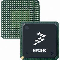
MC68EN360ZQ25VL Freescale Semiconductor, MC68EN360ZQ25VL Datasheet - Page 316

MC68EN360ZQ25VL
Manufacturer Part Number
MC68EN360ZQ25VL
Description
IC MPU QUICC 32BIT 357-PBGA
Manufacturer
Freescale Semiconductor
Datasheets
1.MC68EN302AG20BT.pdf
(8 pages)
2.MC68EN360VR25L.pdf
(14 pages)
3.MC68EN360VR25L.pdf
(2 pages)
4.MC68EN360ZQ25VL.pdf
(962 pages)
Specifications of MC68EN360ZQ25VL
Processor Type
M683xx 32-Bit
Speed
25MHz
Voltage
3.3V
Mounting Type
Surface Mount
Package / Case
357-PBGA
Family Name
M68xxx
Device Core
ColdFire
Device Core Size
32b
Frequency (max)
25MHz
Instruction Set Architecture
RISC
Supply Voltage 1 (typ)
3V
Operating Supply Voltage (max)
3.3V
Operating Supply Voltage (min)
2.7V
Operating Temp Range
0C to 70C
Operating Temperature Classification
Commercial
Mounting
Surface Mount
Pin Count
357
Package Type
BGA
Lead Free Status / RoHS Status
Contains lead / RoHS non-compliant
Features
-
Lead Free Status / Rohs Status
Not Compliant
Available stocks
Company
Part Number
Manufacturer
Quantity
Price
Company:
Part Number:
MC68EN360ZQ25VL
Manufacturer:
Freescale Semiconductor
Quantity:
10 000
- MC68EN302AG20BT PDF datasheet
- MC68EN360VR25L PDF datasheet #2
- MC68EN360VR25L PDF datasheet #3
- MC68EN360ZQ25VL PDF datasheet #4
- Current page: 316 of 962
- Download datasheet (4Mb)
System Integration Module (SIM60)
BACK40—Burst Acknowledge MC68EC040
TRLXQ—Timing Relax
FC3–FC0—Function Code
BA31–BA11—Base Address
6-72
This bit is used to acknowledge a burst cycle to the MC68040. If set, bursts are enabled
in this bank. The QUICC generates address lines 2,3 on the BADDR3–BADDR2 pins.
This bit delays the beginning of the internal QUICC or external QUICC/MC68030-type bus
master cycle to relax the timing constraints on the user. This attribute is useful for slow
peripherals that require additional address setup time. Chip selects are delayed by one
phase, and the cycle is delayed by one clock. For accesses to DRAM, RAS is delayed by
one phase, and CAS and AMUX are delayed by two phases, giving a total cycle increase
of one clock. See Figures 6-16 and 6-17 for timing diagrams of different cases.
This field can be used to specify that accesses with the memory bank be limited to a cer-
tain address space type. These bits are used in conjunction with the FCM3–FCM0 bits in
the OR.
The base address field, the upper 21 bits of each BR, and the function code field are com-
pared to the address on the address bus to determine if a DRAM/SRAM region is being
accessed by an internal QUICC master.
If the SRAM/DRAM region is being accessed by an external master and the WE lines are
not used, then A31–A28 address lines and the BA31–BA28 bits are also used in the com-
parison. If, however, the SRAM/DRAM region is being accessed by an external master
0 = Do not acknowledge burst.
1 = Acknowledge burst; MC68040 bursts are handled by the memory controller for this
0 = Do not relax timing.
1 = Relax timing at the beginning of the cycle. One additional clock cycle is added
bank.
when this bit is set.
CSNT40 is ignored for an SRAM cycle by an external master if
the SYNC bit is cleared. CSNT40 = 1 is not valid for external
DSACK assertion
TRLXQ is ignored for an SRAM cycle by an external master if
the SYNC bit is cleared.
To relax the MC68EC040 cycles, use the TSS40 bit in the GMR.
User should avoid setting both TRLXQ and CSNTQ = 1, when
TCYC = 0. This bit combination will result in a bus cycle without
CS assertion.
Freescale Semiconductor, Inc.
For More Information On This Product,
MC68360 USER’S MANUAL
Go to: www.freescale.com
NOTE
NOTE
Related parts for MC68EN360ZQ25VL
Image
Part Number
Description
Manufacturer
Datasheet
Request
R
Part Number:
Description:
Manufacturer:
Freescale Semiconductor, Inc
Datasheet:
Part Number:
Description:
Manufacturer:
Freescale Semiconductor, Inc
Datasheet:
Part Number:
Description:
Manufacturer:
Freescale Semiconductor, Inc
Datasheet:
Part Number:
Description:
Manufacturer:
Freescale Semiconductor, Inc
Datasheet:
Part Number:
Description:
Manufacturer:
Freescale Semiconductor, Inc
Datasheet:
Part Number:
Description:
Manufacturer:
Freescale Semiconductor, Inc
Datasheet:
Part Number:
Description:
Manufacturer:
Freescale Semiconductor, Inc
Datasheet:
Part Number:
Description:
Manufacturer:
Freescale Semiconductor, Inc
Datasheet:
Part Number:
Description:
Manufacturer:
Freescale Semiconductor, Inc
Datasheet:
Part Number:
Description:
Manufacturer:
Freescale Semiconductor, Inc
Datasheet:
Part Number:
Description:
Manufacturer:
Freescale Semiconductor, Inc
Datasheet:
Part Number:
Description:
Manufacturer:
Freescale Semiconductor, Inc
Datasheet:
Part Number:
Description:
Manufacturer:
Freescale Semiconductor, Inc
Datasheet:
Part Number:
Description:
Manufacturer:
Freescale Semiconductor, Inc
Datasheet:
Part Number:
Description:
Manufacturer:
Freescale Semiconductor, Inc
Datasheet:


