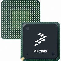
MC68EN360ZQ25VL Freescale Semiconductor, MC68EN360ZQ25VL Datasheet - Page 543

MC68EN360ZQ25VL
Manufacturer Part Number
MC68EN360ZQ25VL
Description
IC MPU QUICC 32BIT 357-PBGA
Manufacturer
Freescale Semiconductor
Datasheets
1.MC68EN302AG20BT.pdf
(8 pages)
2.MC68EN360VR25L.pdf
(14 pages)
3.MC68EN360VR25L.pdf
(2 pages)
4.MC68EN360ZQ25VL.pdf
(962 pages)
Specifications of MC68EN360ZQ25VL
Processor Type
M683xx 32-Bit
Speed
25MHz
Voltage
3.3V
Mounting Type
Surface Mount
Package / Case
357-PBGA
Family Name
M68xxx
Device Core
ColdFire
Device Core Size
32b
Frequency (max)
25MHz
Instruction Set Architecture
RISC
Supply Voltage 1 (typ)
3V
Operating Supply Voltage (max)
3.3V
Operating Supply Voltage (min)
2.7V
Operating Temp Range
0C to 70C
Operating Temperature Classification
Commercial
Mounting
Surface Mount
Pin Count
357
Package Type
BGA
Lead Free Status / RoHS Status
Contains lead / RoHS non-compliant
Features
-
Lead Free Status / Rohs Status
Not Compliant
Available stocks
Company
Part Number
Manufacturer
Quantity
Price
Company:
Part Number:
MC68EN360ZQ25VL
Manufacturer:
Freescale Semiconductor
Quantity:
10 000
- MC68EN302AG20BT PDF datasheet
- MC68EN360VR25L PDF datasheet #2
- MC68EN360VR25L PDF datasheet #3
- MC68EN360ZQ25VL PDF datasheet #4
- Current page: 543 of 962
- Download datasheet (4Mb)
controller is configured with the RTS4, CTS4, and CD4 pins active. The CLK7 pin is used
for both the BISYNC receiver and transmitter.
1. The SDCR (SDMA Configuration Register) should be initialized to $0740, rather than
2. Configure the port A pins to enable the TXD4 and RXD4 pins. Write PAPAR bits 6
3. Configure the port C pins to enable RTS4, CTS4, and CD4. Write PCPAR bit 3 with
4. Configure port A to enable the CLK7 pin. Write PAPAR bit 14 with a one. Write
5. Connect the CLK7 pin to SCC4 using the SI. Write the R4CS bits in SICR to 110.
6. Connect the SCC4 to the NMSI (i.e., its own set of pins). Clear the SC4 bit
7. Write $0740 to the SDCR to initialize the SDMA Configuration Register.
8. Write RBASE and TBASE in the SCC parameter RAM to point to the Rx BD and Tx
9. Program the CR to execute the INIT RX & TX PARAMS command for this channel.
10. Write RFCR with $18 and TFCR with $18 for normal operation.
11. Write MRBLR with the maximum number of bytes per receive buffer. For this case,
12. Write PRCRC with $0000 to comply with CRC16.
13. Write PTCRC with $0000 to comply with CRC16.
14. Clear PAREC for the sake of clarity.
15. Write BSYNC with $8033, assuming a SYNC value of $33.
16. Write BDLE with $8055, assuming a DLE value of $55.
17. Write CHARACTER1–8 with $8000. They are not used.
18. Write RCCM with $E0FF. It is not used.
19. Initialize the Rx BD. Assume the Rx data buffer is at $00001000 in main memory.
20. Initialize the Tx BD. Assume the Tx data buffer is at $00002000 in main memory
being left at its default value of $0000.
and 7 with ones. Write PADIR bits 6 and 7 with zeros. Write PAODR bits 6 and 7
with zeros.
one and bits 10 and 11 with zeros. Write PCDIR bits 3, 10, and 11 with zeros.
Write PCSO bits 10 and 11 with ones.
PADIR bit 14 with a zero.
Write the T4CS bits in SICR to 110.
in the SICR.
BD in the dual-port RAM. Assuming one Rx BD at the beginning of dual-port RAM,
and one Tx BD following that Rx BD, write RBASE with $0000 and TBASE with
$0008.
For instance, to execute this command for SCC1, write $0001 to the CR. This com-
mand causes the RBPTR and TBPTR parameters of the serial channel to be updated
with the new values just programmed into RBASE and TBASE.
assume 16 bytes, so MRBLR = $0010.
Write $B000 to Rx_BD_Status. Write $0000 to Rx_BD_Length (not required—
done for instructional purposes only). Write $00001000 to Rx_BD_Pointer.
and contains five 8-bit characters. Write $BD20 to Tx_BD_Status. Write $0005 to
Freescale Semiconductor, Inc.
For More Information On This Product,
MC68360 USER’S MANUAL
Go to: www.freescale.com
Serial Communication Controllers (SCCs)
Related parts for MC68EN360ZQ25VL
Image
Part Number
Description
Manufacturer
Datasheet
Request
R
Part Number:
Description:
Manufacturer:
Freescale Semiconductor, Inc
Datasheet:
Part Number:
Description:
Manufacturer:
Freescale Semiconductor, Inc
Datasheet:
Part Number:
Description:
Manufacturer:
Freescale Semiconductor, Inc
Datasheet:
Part Number:
Description:
Manufacturer:
Freescale Semiconductor, Inc
Datasheet:
Part Number:
Description:
Manufacturer:
Freescale Semiconductor, Inc
Datasheet:
Part Number:
Description:
Manufacturer:
Freescale Semiconductor, Inc
Datasheet:
Part Number:
Description:
Manufacturer:
Freescale Semiconductor, Inc
Datasheet:
Part Number:
Description:
Manufacturer:
Freescale Semiconductor, Inc
Datasheet:
Part Number:
Description:
Manufacturer:
Freescale Semiconductor, Inc
Datasheet:
Part Number:
Description:
Manufacturer:
Freescale Semiconductor, Inc
Datasheet:
Part Number:
Description:
Manufacturer:
Freescale Semiconductor, Inc
Datasheet:
Part Number:
Description:
Manufacturer:
Freescale Semiconductor, Inc
Datasheet:
Part Number:
Description:
Manufacturer:
Freescale Semiconductor, Inc
Datasheet:
Part Number:
Description:
Manufacturer:
Freescale Semiconductor, Inc
Datasheet:
Part Number:
Description:
Manufacturer:
Freescale Semiconductor, Inc
Datasheet:


