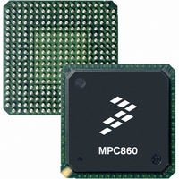
MC68EN360ZQ25VL Freescale Semiconductor, MC68EN360ZQ25VL Datasheet - Page 674

MC68EN360ZQ25VL
Manufacturer Part Number
MC68EN360ZQ25VL
Description
IC MPU QUICC 32BIT 357-PBGA
Manufacturer
Freescale Semiconductor
Datasheets
1.MC68EN302AG20BT.pdf
(8 pages)
2.MC68EN360VR25L.pdf
(14 pages)
3.MC68EN360VR25L.pdf
(2 pages)
4.MC68EN360ZQ25VL.pdf
(962 pages)
Specifications of MC68EN360ZQ25VL
Processor Type
M683xx 32-Bit
Speed
25MHz
Voltage
3.3V
Mounting Type
Surface Mount
Package / Case
357-PBGA
Family Name
M68xxx
Device Core
ColdFire
Device Core Size
32b
Frequency (max)
25MHz
Instruction Set Architecture
RISC
Supply Voltage 1 (typ)
3V
Operating Supply Voltage (max)
3.3V
Operating Supply Voltage (min)
2.7V
Operating Temp Range
0C to 70C
Operating Temperature Classification
Commercial
Mounting
Surface Mount
Pin Count
357
Package Type
BGA
Lead Free Status / RoHS Status
Contains lead / RoHS non-compliant
Features
-
Lead Free Status / Rohs Status
Not Compliant
Available stocks
Company
Part Number
Manufacturer
Quantity
Price
Company:
Part Number:
MC68EN360ZQ25VL
Manufacturer:
Freescale Semiconductor
Quantity:
10 000
- MC68EN302AG20BT PDF datasheet
- MC68EN360VR25L PDF datasheet #2
- MC68EN360VR25L PDF datasheet #3
- MC68EN360ZQ25VL PDF datasheet #4
- Current page: 674 of 962
- Download datasheet (4Mb)
Parallel Interface Port (PIP)
TXE—Transmit Error
CHR—Character Transmitted
TX—Tx Buffer
7.13.8.12 CENTRONICS CHANNEL RECEPTION. The Centronics receiver supports the
same general data structure that is used by the SCCs for other protocols. Upon receiving a
character from the Centronics interface, the receiver will check if the current buffer descrip-
tor (BD) in the Centronics receiver BD table is ready for use. If the BD is ready, the Centron-
ics receiver will compare the character against a user defined control character table. If no
match was found, the character will be written to the BD’s associated buffer. If a match was
found, the character will be either written to the receive buffer (upon which the buffer is
closed and a new receive buffer taken) or rejected, depending on the R bit in the Control
Character Table. If rejected, the character is written to the Received Control Character Reg-
ister (RCCR) in internal RAM and a maskable interrupt is generated. A maskable interrupt
will be generated at the completion of the BD processing. A single received data frame may
span several BDs.
For each transfer, the Centronics controller will generate ACK and BUSY handshake signals
on the Centronics interface. The ACK pulse width and the timing of BUSY with respect to
the ACK signal are determined by the setting in the PIP Timing Parameter Register (PTPR).
7.13.8.13 CENTRONICS RECEIVER MEMORY MAP. When configured to operate in Cen-
tronics receive mode, the QUICC overlays the structure illustrated in Table 7-17 with the
SMC2 parameter RAM area.
7-350
An error condition was detected. This error status is reported in the buffer descriptor.
Acknowledgment that the last character was strobed into the receiver input latch (STB
was asserted by the transmitter) and a new character was written to the data register.
A buffer has been transmitted over the Centronics channel. This bit is set only after the
last character of the buffer was strobed into the receiver input latch (STB was asserted by
the transmitter).
PIP Base+00
PIP Base+02
PIP Base+04
PIP Base+05
PIP Base+06
PIP Base+08
PIP Base+0C
PIP Base+10
Address
Table 7-18. Centronics Receiver Parameter RAM
RBASE
Res
CFCR
Res
MRBLR
RSTATE
R_PTR
RBPTR
Freescale Semiconductor, Inc.
7
–
Name
For More Information On This Product,
6
–
MC68360 USER’S MANUAL
Go to: www.freescale.com
Word
Word
Byte
Byte
Word
Long
Long
Word
5
–
Width
TXE
4
3
–
Rx Buffer Descriptors Base Address
Reserved
Centronics Function Code
Reserved
Maximum Receive Buffer Length
Rx Internal State
Rx Internal Data Pointer
Rx Buffer Descriptor Pointer
2
–
CHR
1
Description
TX
0
Related parts for MC68EN360ZQ25VL
Image
Part Number
Description
Manufacturer
Datasheet
Request
R
Part Number:
Description:
Manufacturer:
Freescale Semiconductor, Inc
Datasheet:
Part Number:
Description:
Manufacturer:
Freescale Semiconductor, Inc
Datasheet:
Part Number:
Description:
Manufacturer:
Freescale Semiconductor, Inc
Datasheet:
Part Number:
Description:
Manufacturer:
Freescale Semiconductor, Inc
Datasheet:
Part Number:
Description:
Manufacturer:
Freescale Semiconductor, Inc
Datasheet:
Part Number:
Description:
Manufacturer:
Freescale Semiconductor, Inc
Datasheet:
Part Number:
Description:
Manufacturer:
Freescale Semiconductor, Inc
Datasheet:
Part Number:
Description:
Manufacturer:
Freescale Semiconductor, Inc
Datasheet:
Part Number:
Description:
Manufacturer:
Freescale Semiconductor, Inc
Datasheet:
Part Number:
Description:
Manufacturer:
Freescale Semiconductor, Inc
Datasheet:
Part Number:
Description:
Manufacturer:
Freescale Semiconductor, Inc
Datasheet:
Part Number:
Description:
Manufacturer:
Freescale Semiconductor, Inc
Datasheet:
Part Number:
Description:
Manufacturer:
Freescale Semiconductor, Inc
Datasheet:
Part Number:
Description:
Manufacturer:
Freescale Semiconductor, Inc
Datasheet:
Part Number:
Description:
Manufacturer:
Freescale Semiconductor, Inc
Datasheet:


