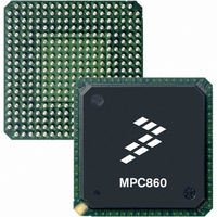
MC68EN360ZQ25VL Freescale Semiconductor, MC68EN360ZQ25VL Datasheet - Page 272

MC68EN360ZQ25VL
Manufacturer Part Number
MC68EN360ZQ25VL
Description
IC MPU QUICC 32BIT 357-PBGA
Manufacturer
Freescale Semiconductor
Datasheets
1.MC68EN302AG20BT.pdf
(8 pages)
2.MC68EN360VR25L.pdf
(14 pages)
3.MC68EN360VR25L.pdf
(2 pages)
4.MC68EN360ZQ25VL.pdf
(962 pages)
Specifications of MC68EN360ZQ25VL
Processor Type
M683xx 32-Bit
Speed
25MHz
Voltage
3.3V
Mounting Type
Surface Mount
Package / Case
357-PBGA
Family Name
M68xxx
Device Core
ColdFire
Device Core Size
32b
Frequency (max)
25MHz
Instruction Set Architecture
RISC
Supply Voltage 1 (typ)
3V
Operating Supply Voltage (max)
3.3V
Operating Supply Voltage (min)
2.7V
Operating Temp Range
0C to 70C
Operating Temperature Classification
Commercial
Mounting
Surface Mount
Pin Count
357
Package Type
BGA
Lead Free Status / RoHS Status
Contains lead / RoHS non-compliant
Features
-
Lead Free Status / Rohs Status
Not Compliant
Available stocks
Company
Part Number
Manufacturer
Quantity
Price
Company:
Part Number:
MC68EN360ZQ25VL
Manufacturer:
Freescale Semiconductor
Quantity:
10 000
- MC68EN302AG20BT PDF datasheet
- MC68EN360VR25L PDF datasheet #2
- MC68EN360VR25L PDF datasheet #3
- MC68EN360ZQ25VL PDF datasheet #4
- Current page: 272 of 962
- Download datasheet (4Mb)
System Integration Module (SIM60)
For each address space bit:
V—Valid
MBAR can be read using the following code. Register D0 will contain the value of MBAR.
6-28
4. AS5—mask supervisor data address space (FC3–FC0=0101)
5. AS4—mask Motorola reserved address space (FC3–FC0=0100)
6. AS3—mask user reserved address space (FC3–FC0=0011)
7. AS2—mask user program address space (FC3–FC0=0010)
8. AS1—mask user data address space (FC3–FC0=0001)
9. AS0—mask Motorola reserved address space (FC3–FC0=0000)
The address space bits for 040 type MPU are:
1. AS8—no relevance for 040 cycles
2. AS7—acknowledge access (TT1-TT0=11)
3. AS6—supervisor code access (TT1-TT0=00, TM2-TM0=110)
4. AS5—supervisor data access (TT1-TT0=00, TM2-TM0=101)
5. AS4—MMU table search code access (TT1-TT0=00, TM2-TM0=100)
6. AS3—MMU table search data access (TT1-TT0=00, TM2-TM0=011)
7. AS2—user code access (TT1-TT0=00, TM2-TM0=010)
8. AS1—user data access (TT1-TT0=00, TM2-TM0=001)
9. AS0—data cache push access (TT1-TT0=00, TM2-TM0=000)
This bit indicates when the contents of the MBAR are valid. The base address value is not
used; therefore, all internal module registers are not accessible until the V-bit is set.
1 = Mask this address space from the internal module selection. The bus cycle goes
0 = Decode for the internal module block.
0 = Contents not valid.
1 = Contents valid.
external.
The user should mask off AS7, AS4, AS3 and AS1 to prevent
unwanted access to the QUICC internal dual port RAM (DPR).
For example, AS7 should be masked out so that the IACK cycle
will not cause an access to the DPR.
When working in the CPU enable mode, an access to this regis-
ter does not affect external space since the cycle is not run ex-
ternally.
Freescale Semiconductor, Inc.
For More Information On This Product,
MC68360 USER’S MANUAL
Go to: www.freescale.com
NOTE
NOTE
Related parts for MC68EN360ZQ25VL
Image
Part Number
Description
Manufacturer
Datasheet
Request
R
Part Number:
Description:
Manufacturer:
Freescale Semiconductor, Inc
Datasheet:
Part Number:
Description:
Manufacturer:
Freescale Semiconductor, Inc
Datasheet:
Part Number:
Description:
Manufacturer:
Freescale Semiconductor, Inc
Datasheet:
Part Number:
Description:
Manufacturer:
Freescale Semiconductor, Inc
Datasheet:
Part Number:
Description:
Manufacturer:
Freescale Semiconductor, Inc
Datasheet:
Part Number:
Description:
Manufacturer:
Freescale Semiconductor, Inc
Datasheet:
Part Number:
Description:
Manufacturer:
Freescale Semiconductor, Inc
Datasheet:
Part Number:
Description:
Manufacturer:
Freescale Semiconductor, Inc
Datasheet:
Part Number:
Description:
Manufacturer:
Freescale Semiconductor, Inc
Datasheet:
Part Number:
Description:
Manufacturer:
Freescale Semiconductor, Inc
Datasheet:
Part Number:
Description:
Manufacturer:
Freescale Semiconductor, Inc
Datasheet:
Part Number:
Description:
Manufacturer:
Freescale Semiconductor, Inc
Datasheet:
Part Number:
Description:
Manufacturer:
Freescale Semiconductor, Inc
Datasheet:
Part Number:
Description:
Manufacturer:
Freescale Semiconductor, Inc
Datasheet:
Part Number:
Description:
Manufacturer:
Freescale Semiconductor, Inc
Datasheet:


