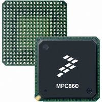
MC68EN360ZQ25VL Freescale Semiconductor, MC68EN360ZQ25VL Datasheet - Page 61

MC68EN360ZQ25VL
Manufacturer Part Number
MC68EN360ZQ25VL
Description
IC MPU QUICC 32BIT 357-PBGA
Manufacturer
Freescale Semiconductor
Datasheets
1.MC68EN302AG20BT.pdf
(8 pages)
2.MC68EN360VR25L.pdf
(14 pages)
3.MC68EN360VR25L.pdf
(2 pages)
4.MC68EN360ZQ25VL.pdf
(962 pages)
Specifications of MC68EN360ZQ25VL
Processor Type
M683xx 32-Bit
Speed
25MHz
Voltage
3.3V
Mounting Type
Surface Mount
Package / Case
357-PBGA
Family Name
M68xxx
Device Core
ColdFire
Device Core Size
32b
Frequency (max)
25MHz
Instruction Set Architecture
RISC
Supply Voltage 1 (typ)
3V
Operating Supply Voltage (max)
3.3V
Operating Supply Voltage (min)
2.7V
Operating Temp Range
0C to 70C
Operating Temperature Classification
Commercial
Mounting
Surface Mount
Pin Count
357
Package Type
BGA
Lead Free Status / RoHS Status
Contains lead / RoHS non-compliant
Features
-
Lead Free Status / Rohs Status
Not Compliant
Available stocks
Company
Part Number
Manufacturer
Quantity
Price
Company:
Part Number:
MC68EN360ZQ25VL
Manufacturer:
Freescale Semiconductor
Quantity:
10 000
- MC68EN302AG20BT PDF datasheet
- MC68EN360VR25L PDF datasheet #2
- MC68EN360VR25L PDF datasheet #3
- MC68EN360ZQ25VL PDF datasheet #4
- Current page: 61 of 962
- Download datasheet (4Mb)
2.1.14 Power Signals
The following signals are used for power and ground to the QUICC.
2.1.14.1 VCCSYN AND GNDSYN. These pins provide power and ground to the clock syn-
thesizer. They should be bypassed to each other with a 0.1- F capacitor. See the system
clock generation description in Section 6 System Integration Module (SIM60) for more
details.
2.1.14.2 VCCCLK AND GNDCLK. These pins provide power and ground to the clock out-
put pins (CLKO1 and CLKO2). They should be bypassed to each other with a 0.1- F capac-
itor. See the system clock generation description in Section 6 System Integration Module
(SIM60) for more detail.
2.1.14.3 GNDS1 AND GNDS2. These two pins are special ground pins that, if used prop-
erly, allow more aggressive timing to be provided on certain system bus pins. These pins
include AS, CASx, and IPIPE. Section 10 Electrical Characteristics already shows the
aggressive timing; the user does not need to modify any values in the section. GNDS1 and
GNDS2 should be connected to a quiet ground source or to a low-noise ground plane.
2.1.14.4 VCC AND GND. These pins are the rest of the power and ground connections for
the QUICC.
2.1.14.5 NC4–NC1. These four pins should not be connected on the QUICC package. They
are reserved for future enhancements.
CONFIG2/
FREEZE
0
0
0
0
1
1
1
1
Configuration Pins
CONFIG1/
All CONFIG pins do have an internal pull-up resistor during re-
set. If a configuration other than the default (CONFIG2-1 = 111)
is desired, these pins should be driven by an active open collec-
tor device during the assertion of RESETH.
BCLRO
0
0
1
1
0
0
1
1
Freescale Semiconductor, Inc.
CONFIG0/
For More Information On This Product,
RMC
0
1
0
1
0
1
0
1
Table 2-6. Initial Configuration
MC68360 USER’S MANUAL
Go to: www.freescale.com
Slave mode; global CS 8-bit size; MBAR at $003FF00.
Slave mode; global CS 32-bit size; MBAR at $003FF00; not MC68040 com-
panion mode; BR output, BG input.
Slave mode; global CS 16-bit size; MBAR at $003FF00.
MC68040 companion mode; global CS 32-bit size; MBAR at $003FF00; BR
input, BG output.
CPU enabled; global CS 32-bit size; MBAR at $003FF00.
CPU enabled; global CS 16-bit size; MBAR at $003FF00.
Slave mode; global CS disabled; MBAR at $003FF04.
CPU enabled; global CS 8-bit size; MBAR at $003FF00. (Default)
NOTE
Result
Signal Descriptions
Related parts for MC68EN360ZQ25VL
Image
Part Number
Description
Manufacturer
Datasheet
Request
R
Part Number:
Description:
Manufacturer:
Freescale Semiconductor, Inc
Datasheet:
Part Number:
Description:
Manufacturer:
Freescale Semiconductor, Inc
Datasheet:
Part Number:
Description:
Manufacturer:
Freescale Semiconductor, Inc
Datasheet:
Part Number:
Description:
Manufacturer:
Freescale Semiconductor, Inc
Datasheet:
Part Number:
Description:
Manufacturer:
Freescale Semiconductor, Inc
Datasheet:
Part Number:
Description:
Manufacturer:
Freescale Semiconductor, Inc
Datasheet:
Part Number:
Description:
Manufacturer:
Freescale Semiconductor, Inc
Datasheet:
Part Number:
Description:
Manufacturer:
Freescale Semiconductor, Inc
Datasheet:
Part Number:
Description:
Manufacturer:
Freescale Semiconductor, Inc
Datasheet:
Part Number:
Description:
Manufacturer:
Freescale Semiconductor, Inc
Datasheet:
Part Number:
Description:
Manufacturer:
Freescale Semiconductor, Inc
Datasheet:
Part Number:
Description:
Manufacturer:
Freescale Semiconductor, Inc
Datasheet:
Part Number:
Description:
Manufacturer:
Freescale Semiconductor, Inc
Datasheet:
Part Number:
Description:
Manufacturer:
Freescale Semiconductor, Inc
Datasheet:
Part Number:
Description:
Manufacturer:
Freescale Semiconductor, Inc
Datasheet:


