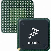
MC68EN360ZQ25VL Freescale Semiconductor, MC68EN360ZQ25VL Datasheet - Page 205

MC68EN360ZQ25VL
Manufacturer Part Number
MC68EN360ZQ25VL
Description
IC MPU QUICC 32BIT 357-PBGA
Manufacturer
Freescale Semiconductor
Datasheets
1.MC68EN302AG20BT.pdf
(8 pages)
2.MC68EN360VR25L.pdf
(14 pages)
3.MC68EN360VR25L.pdf
(2 pages)
4.MC68EN360ZQ25VL.pdf
(962 pages)
Specifications of MC68EN360ZQ25VL
Processor Type
M683xx 32-Bit
Speed
25MHz
Voltage
3.3V
Mounting Type
Surface Mount
Package / Case
357-PBGA
Family Name
M68xxx
Device Core
ColdFire
Device Core Size
32b
Frequency (max)
25MHz
Instruction Set Architecture
RISC
Supply Voltage 1 (typ)
3V
Operating Supply Voltage (max)
3.3V
Operating Supply Voltage (min)
2.7V
Operating Temp Range
0C to 70C
Operating Temperature Classification
Commercial
Mounting
Surface Mount
Pin Count
357
Package Type
BGA
Lead Free Status / RoHS Status
Contains lead / RoHS non-compliant
Features
-
Lead Free Status / Rohs Status
Not Compliant
Available stocks
Company
Part Number
Manufacturer
Quantity
Price
Company:
Part Number:
MC68EN360ZQ25VL
Manufacturer:
Freescale Semiconductor
Quantity:
10 000
- MC68EN302AG20BT PDF datasheet
- MC68EN360VR25L PDF datasheet #2
- MC68EN360VR25L PDF datasheet #3
- MC68EN360ZQ25VL PDF datasheet #4
- Current page: 205 of 962
- Download datasheet (4Mb)
Freescale Semiconductor, Inc.
CPU32+
5.6.2.5 BDM REGISTERS. BDM processing uses three special-purpose registers to track
program context during development. A description of each register follows.
5.6.2.5.1 Fault Address Register (FAR). The FAR contains the address of the faulting bus
cycle immediately following a bus or address error. This address remains available until
overwritten by a subsequent bus cycle. Following a double bus fault, the FAR contains the
address of the last bus cycle. The address of the first fault (if one occurred) is not visible to
the user.
5.6.2.5.2 Return Program Counter (RPC). The RPC points to the location where fetching
will commence after transition from BDM to normal mode. This register should be accessed
to change the flow of a program under development. Changing the RPC to an odd value will
cause an address error when normal mode prefetching begins.
5.6.2.5.3 Current Instruction Program Counter (PCC). The PCC holds a pointer to the
first word of the last instruction executed prior to transition into BDM. Due to instruction pipe-
lining, the instruction pointed to may not be the instruction that caused the transition. An
example is a breakpoint on a released write. The bus cycle may overlap as many as two
subsequent instructions before stalling the instruction sequencer. A BKPT asserted during
this cycle will not be acknowledged until the end of the instruction executing at completion
of the bus cycle. PCC will contain $00000001 if BDM is entered via a double bus fault imme-
diately out of reset.
5.6.2.6 RETURNING FROM BDM. BDM is terminated when a resume execution (GO) or
call user code (CALL) command is received. Both GO and CALL flush the instruction pipe-
line and prefetch instructions from the location pointed to by the RPC.
The return PC and the memory space referred to by the SR SUPV bit reflect any changes
made during BDM. FREEZE is negated prior to initiating the first prefetch. Upon negation of
FREEZE, the serial subsystem is disabled, and the signals revert to IPIPE and IFETCH
functionality.
5.6.2.7 SERIAL INTERFACE. Communication with the CPU32+ during BDM occurs via a
dedicated serial interface, which shares pins with other development features. The BKPT
signal becomes the DSCLK; DSI is received on IFETCH, and DSO is transmitted on IPIPE.
The serial interface uses a full-duplex synchronous protocol similar to the serial peripheral
interface (SPI) protocol. The development system serves as the master of the serial link
since it is responsible for the generation of DSCLK. If DSCLK is derived from the CPU32+
system clock, development system serial logic is unhindered by the operating frequency of
the target processor. Operable frequency range of the serial clock is from DC to one-half the
processor system clock frequency
The serial interface operates in full-duplex mode—i.e., data is transmitted and received
simultaneously by both master and slave devices. In general, data transitions occur on the
falling edge of DSCLK and are stable by the following rising edge of DSCLK. Data is trans-
mitted MSB first and is latched on the rising edge of DSCLK.
MC68360 USER’S MANUAL
For More Information On This Product,
Go to: www.freescale.com
Related parts for MC68EN360ZQ25VL
Image
Part Number
Description
Manufacturer
Datasheet
Request
R
Part Number:
Description:
Manufacturer:
Freescale Semiconductor, Inc
Datasheet:
Part Number:
Description:
Manufacturer:
Freescale Semiconductor, Inc
Datasheet:
Part Number:
Description:
Manufacturer:
Freescale Semiconductor, Inc
Datasheet:
Part Number:
Description:
Manufacturer:
Freescale Semiconductor, Inc
Datasheet:
Part Number:
Description:
Manufacturer:
Freescale Semiconductor, Inc
Datasheet:
Part Number:
Description:
Manufacturer:
Freescale Semiconductor, Inc
Datasheet:
Part Number:
Description:
Manufacturer:
Freescale Semiconductor, Inc
Datasheet:
Part Number:
Description:
Manufacturer:
Freescale Semiconductor, Inc
Datasheet:
Part Number:
Description:
Manufacturer:
Freescale Semiconductor, Inc
Datasheet:
Part Number:
Description:
Manufacturer:
Freescale Semiconductor, Inc
Datasheet:
Part Number:
Description:
Manufacturer:
Freescale Semiconductor, Inc
Datasheet:
Part Number:
Description:
Manufacturer:
Freescale Semiconductor, Inc
Datasheet:
Part Number:
Description:
Manufacturer:
Freescale Semiconductor, Inc
Datasheet:
Part Number:
Description:
Manufacturer:
Freescale Semiconductor, Inc
Datasheet:
Part Number:
Description:
Manufacturer:
Freescale Semiconductor, Inc
Datasheet:


