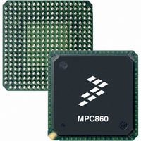
MC68EN360ZQ25VL Freescale Semiconductor, MC68EN360ZQ25VL Datasheet - Page 758

MC68EN360ZQ25VL
Manufacturer Part Number
MC68EN360ZQ25VL
Description
IC MPU QUICC 32BIT 357-PBGA
Manufacturer
Freescale Semiconductor
Datasheets
1.MC68EN302AG20BT.pdf
(8 pages)
2.MC68EN360VR25L.pdf
(14 pages)
3.MC68EN360VR25L.pdf
(2 pages)
4.MC68EN360ZQ25VL.pdf
(962 pages)
Specifications of MC68EN360ZQ25VL
Processor Type
M683xx 32-Bit
Speed
25MHz
Voltage
3.3V
Mounting Type
Surface Mount
Package / Case
357-PBGA
Family Name
M68xxx
Device Core
ColdFire
Device Core Size
32b
Frequency (max)
25MHz
Instruction Set Architecture
RISC
Supply Voltage 1 (typ)
3V
Operating Supply Voltage (max)
3.3V
Operating Supply Voltage (min)
2.7V
Operating Temp Range
0C to 70C
Operating Temperature Classification
Commercial
Mounting
Surface Mount
Pin Count
357
Package Type
BGA
Lead Free Status / RoHS Status
Contains lead / RoHS non-compliant
Features
-
Lead Free Status / Rohs Status
Not Compliant
Available stocks
Company
Part Number
Manufacturer
Quantity
Price
Company:
Part Number:
MC68EN360ZQ25VL
Manufacturer:
Freescale Semiconductor
Quantity:
10 000
- MC68EN302AG20BT PDF datasheet
- MC68EN360VR25L PDF datasheet #2
- MC68EN360VR25L PDF datasheet #3
- MC68EN360ZQ25VL PDF datasheet #4
- Current page: 758 of 962
- Download datasheet (4Mb)
Applications
dled differently. See 9.4.2 Memory Interfaces.) To provide dynamic bus sizing, the MC68150
device may be added to the design shown here.
Parity is supported for both SRAM and DRAM arrays using the four-byte parity lines
PRTY3–PRTY0. When a parity error occurs, the error indication on the PERR pin causes
the QUICC to generate a level 5 interrupt to the MC68EC040. (Level 7 has already been
used for the breakpoint generation interrupt.) The parity error timing is not fast enough to
allow an MC68EC040 bus error to be generated on the bus cycle that generated a parity
error.
The QUICC supports MC68EC040 bursting using the BADD3–BADD2 pins. These pins nor-
mally reflect the values on A3–A2, but, in the case of a burst, are used to increment the
address to the memory array. If the memory devices already support MC68EC040 bursting
internally, the BADD3–BADD2 pins are not required.
The DRAM arrays require the four CAS3–CAS0 pins. Also, since an external address mul-
tiplexer is used, the AMUX pin is required to select between rows and columns. If, however,
the user's configuration does not require DRAM, the AMUX pin can be used as an OE pin
instead. This would save an inverter in a number of memory arrays.
The QUICC also provides four write enable (WEx) pins to select the correct byte during write
operations.
9.4.2.2 REGULAR EPROM. Figure 9-9 shows the glueless interface to standard EPROM
in the system. The assumption is made that only the MC68EC040 will access this array. No
bursting capability is used. The CONFIG2–CONFIG0 pins are configured to initialize the
system to slave mode, CS0 operating on a 32-bit port at reset, the MBAR at its normal loca-
tion, and MC68040 companion mode.
It would have been possible to use 16-bit-wide EPROM to reduce the chip count, if desired.
(See 9.4.2.3 Burst EPROM. for an example.)
9.4.2.3 BURST EPROM. Figure 9-10 shows the glueless interface to two burst EPROMs
available from National Semiconductor. These devices support a glueless interface to the
MC68040. In this design, the assumption is made that only the MC68EC040 will access this
array.
9-38
Many memory arrays show an inverter on the R/W pin to create
the OE signal. When using multiple memory arrays, it is possible
to share one inverter between multiple memory arrays; however,
this configuration is not shown.
Freescale Semiconductor, Inc.
For More Information On This Product,
MC68360 USER’S MANUAL
Go to: www.freescale.com
NOTE
Related parts for MC68EN360ZQ25VL
Image
Part Number
Description
Manufacturer
Datasheet
Request
R
Part Number:
Description:
Manufacturer:
Freescale Semiconductor, Inc
Datasheet:
Part Number:
Description:
Manufacturer:
Freescale Semiconductor, Inc
Datasheet:
Part Number:
Description:
Manufacturer:
Freescale Semiconductor, Inc
Datasheet:
Part Number:
Description:
Manufacturer:
Freescale Semiconductor, Inc
Datasheet:
Part Number:
Description:
Manufacturer:
Freescale Semiconductor, Inc
Datasheet:
Part Number:
Description:
Manufacturer:
Freescale Semiconductor, Inc
Datasheet:
Part Number:
Description:
Manufacturer:
Freescale Semiconductor, Inc
Datasheet:
Part Number:
Description:
Manufacturer:
Freescale Semiconductor, Inc
Datasheet:
Part Number:
Description:
Manufacturer:
Freescale Semiconductor, Inc
Datasheet:
Part Number:
Description:
Manufacturer:
Freescale Semiconductor, Inc
Datasheet:
Part Number:
Description:
Manufacturer:
Freescale Semiconductor, Inc
Datasheet:
Part Number:
Description:
Manufacturer:
Freescale Semiconductor, Inc
Datasheet:
Part Number:
Description:
Manufacturer:
Freescale Semiconductor, Inc
Datasheet:
Part Number:
Description:
Manufacturer:
Freescale Semiconductor, Inc
Datasheet:
Part Number:
Description:
Manufacturer:
Freescale Semiconductor, Inc
Datasheet:


