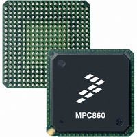
MC68EN360ZQ25VL Freescale Semiconductor, MC68EN360ZQ25VL Datasheet - Page 752

MC68EN360ZQ25VL
Manufacturer Part Number
MC68EN360ZQ25VL
Description
IC MPU QUICC 32BIT 357-PBGA
Manufacturer
Freescale Semiconductor
Datasheets
1.MC68EN302AG20BT.pdf
(8 pages)
2.MC68EN360VR25L.pdf
(14 pages)
3.MC68EN360VR25L.pdf
(2 pages)
4.MC68EN360ZQ25VL.pdf
(962 pages)
Specifications of MC68EN360ZQ25VL
Processor Type
M683xx 32-Bit
Speed
25MHz
Voltage
3.3V
Mounting Type
Surface Mount
Package / Case
357-PBGA
Family Name
M68xxx
Device Core
ColdFire
Device Core Size
32b
Frequency (max)
25MHz
Instruction Set Architecture
RISC
Supply Voltage 1 (typ)
3V
Operating Supply Voltage (max)
3.3V
Operating Supply Voltage (min)
2.7V
Operating Temp Range
0C to 70C
Operating Temperature Classification
Commercial
Mounting
Surface Mount
Pin Count
357
Package Type
BGA
Lead Free Status / RoHS Status
Contains lead / RoHS non-compliant
Features
-
Lead Free Status / Rohs Status
Not Compliant
Available stocks
Company
Part Number
Manufacturer
Quantity
Price
Company:
Part Number:
MC68EN360ZQ25VL
Manufacturer:
Freescale Semiconductor
Quantity:
10 000
- MC68EN302AG20BT PDF datasheet
- MC68EN360VR25L PDF datasheet #2
- MC68EN360VR25L PDF datasheet #3
- MC68EN360ZQ25VL PDF datasheet #4
- Current page: 752 of 962
- Download datasheet (4Mb)
Applications
The following paragraphs discuss both the hardware and software issues concerning this
solution in a system that contains one MC68EC040 and one QUICC. It is also possible to
interface more than one QUICC to an MC68EC040. This topic is discussed briefly in para-
graph 9.4.4 Interfacing Multiple QUICCs to an MC68EC040.
9.4.1 MC68EC040 to QUICC Interface
The following paragraphs discuss the hardware and software issues relating to the connec-
tion between the MC68EC040 and the QUICC. The features of the QUICC that may be used
to assist the MC68EC040 are also detailed. Reference Figure 9-8 during this discussion.
9.4.1.1 MC68EC040 READS AND WRITES TO QUICC. The basic connection is made
through the data and address bus. All 32 data lines are routed between devices, which is
required for the connection. In slave mode, the QUICC is not allowed to use its 16-bit data
bus mode.
Twenty-eight address lines are routed between devices, giving a 256-Mbyte shared address
capability. It is possible to share all 32 address lines between devices, but the QUICC would
then lose its write enable lines (WE3–WE0). These lines are very useful in memory inter-
faces, and are used in this application.
In the MC68040 companion mode, the QUICC provides a number of signal changes to
accommodate the MC68EC040. These changes allow direct connection between the
MC68EC040 and the QUICC. These QUICC signals carry the same names as the compa-
rable MC68EC040 signal: transfer start (TS), transfer acknowledge (TA), transfer exception
acknowledge (TEA), transfer burst inhibit (TBI), transfer type (TT1–TT0), and transfer mode
(TM2–TM0).
In addition, the QUICC R/W and SIZ1–SIZ0 signals that are used in all configurations are
directly connected to the MC68EC040. When the MC68EC040 begins an access, the
QUICC interprets the SIZx pins, using the MC68EC040 encoding rather than the QUICC
encoding.
9-32
The QUICC monitors the address bus in slave mode to perform
memory controller functions. Therefore, the user should never
gate 040 bus control signals (i.e., TA, TS signals) between 040
and QUICC, even if the address output by the 040 is not con-
trolled or used by the QUICC.
Freescale Semiconductor, Inc.
For More Information On This Product,
MC68360 USER’S MANUAL
Go to: www.freescale.com
NOTE
Related parts for MC68EN360ZQ25VL
Image
Part Number
Description
Manufacturer
Datasheet
Request
R
Part Number:
Description:
Manufacturer:
Freescale Semiconductor, Inc
Datasheet:
Part Number:
Description:
Manufacturer:
Freescale Semiconductor, Inc
Datasheet:
Part Number:
Description:
Manufacturer:
Freescale Semiconductor, Inc
Datasheet:
Part Number:
Description:
Manufacturer:
Freescale Semiconductor, Inc
Datasheet:
Part Number:
Description:
Manufacturer:
Freescale Semiconductor, Inc
Datasheet:
Part Number:
Description:
Manufacturer:
Freescale Semiconductor, Inc
Datasheet:
Part Number:
Description:
Manufacturer:
Freescale Semiconductor, Inc
Datasheet:
Part Number:
Description:
Manufacturer:
Freescale Semiconductor, Inc
Datasheet:
Part Number:
Description:
Manufacturer:
Freescale Semiconductor, Inc
Datasheet:
Part Number:
Description:
Manufacturer:
Freescale Semiconductor, Inc
Datasheet:
Part Number:
Description:
Manufacturer:
Freescale Semiconductor, Inc
Datasheet:
Part Number:
Description:
Manufacturer:
Freescale Semiconductor, Inc
Datasheet:
Part Number:
Description:
Manufacturer:
Freescale Semiconductor, Inc
Datasheet:
Part Number:
Description:
Manufacturer:
Freescale Semiconductor, Inc
Datasheet:
Part Number:
Description:
Manufacturer:
Freescale Semiconductor, Inc
Datasheet:


