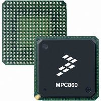
MC68EN360ZQ25VL Freescale Semiconductor, MC68EN360ZQ25VL Datasheet - Page 365

MC68EN360ZQ25VL
Manufacturer Part Number
MC68EN360ZQ25VL
Description
IC MPU QUICC 32BIT 357-PBGA
Manufacturer
Freescale Semiconductor
Datasheets
1.MC68EN302AG20BT.pdf
(8 pages)
2.MC68EN360VR25L.pdf
(14 pages)
3.MC68EN360VR25L.pdf
(2 pages)
4.MC68EN360ZQ25VL.pdf
(962 pages)
Specifications of MC68EN360ZQ25VL
Processor Type
M683xx 32-Bit
Speed
25MHz
Voltage
3.3V
Mounting Type
Surface Mount
Package / Case
357-PBGA
Family Name
M68xxx
Device Core
ColdFire
Device Core Size
32b
Frequency (max)
25MHz
Instruction Set Architecture
RISC
Supply Voltage 1 (typ)
3V
Operating Supply Voltage (max)
3.3V
Operating Supply Voltage (min)
2.7V
Operating Temp Range
0C to 70C
Operating Temperature Classification
Commercial
Mounting
Surface Mount
Pin Count
357
Package Type
BGA
Lead Free Status / RoHS Status
Contains lead / RoHS non-compliant
Features
-
Lead Free Status / Rohs Status
Not Compliant
Available stocks
Company
Part Number
Manufacturer
Quantity
Price
Company:
Part Number:
MC68EN360ZQ25VL
Manufacturer:
Freescale Semiconductor
Quantity:
10 000
- MC68EN302AG20BT PDF datasheet
- MC68EN360VR25L PDF datasheet #2
- MC68EN360VR25L PDF datasheet #3
- MC68EN360ZQ25VL PDF datasheet #4
- Current page: 365 of 962
- Download datasheet (4Mb)
determined by the ECO bit in the CMR. The DACKx timing is similar to the timing of the AS
pin. Thus, DACKx is the acknowledgment of the original burst request given on the DREQx
pin.
During each access to the device (i.e., DACKx is asserted), the IDMA will sample DREQx
at the S3 falling edge of the bus cycle to determine whether the burst should continue. If
DREQx is asserted, the burst continues. If DREQx is negated, the burst ceases, and another
operand transfer to/from the device does not occur until DREQx is asserted again. If DREQx
is negated, but not in time to stop the burst on this bus cycle, one additional bus cycle to the
device will occur before the IDMA stops the burst.
The previous paragraphs discuss the general rules; however, important special cases are
discussed in the following points:
1. The sample point at the S3 falling edge means the last S3 before the S4 edge that
2. The sample point at S3 assumes that the required setup time is met, as defined in Sec-
3. If SRM is cleared in the CMR (default condition), then DREQx is synchronized inter-
4. If operand packing is performed, the user does not need to negate DREQx on any par-
5. If operand packing is performed and the peripheral is the source and DREQx is negat-
6. If the access to the device is a fast termination access, the DREQx negation timing
completes the cycle. Thus, if wait states are inserted in the bus cycle, the sample point
is later in the cycle.
tion 10 Electrical Characteristics.
nally before it is used; therefore, DREQx must be negated one clock earlier than the
S3 falling edge to be recognized on that cycle.
ticular access to the device. For instance, if the source is a 32-bit memory and the des-
tination is an 8-bit peripheral, DREQx can be negated on the first, second, third, or
fourth byte access to the peripheral. In each case, if the DREQx negation timings are
met, the IDMA will stop accessing the peripheral immediately with no additional bus
cycles to the peripheral. Accesses to the peripheral will resume when DREQx is as-
serted.
ed to stop the burst, the IDMA will attempt to empty the contents of the DHR (by per-
forming one additional write cycle to memory) before giving up the bus. The IDMA
attempts to minimize the contents of the DHR between burst requests.
cannot be met, and one additional bus cycle will always occur to the device before the
burst stops.
Because DACKx timing is similar to AS timing, the user typically
uses the assertion of DACKx as an indication that DREQx is ne-
later than DSACKx because DSACKx pins are also sampled at
falling S3 to determine the end of the bus cycle.
gated.
To meet the S3 sampling time, DREQx should be negated no
Freescale Semiconductor, Inc.
For More Information On This Product,
MC68360 USER’S MANUAL
Go to: www.freescale.com
NOTES
IDMA Channels
Related parts for MC68EN360ZQ25VL
Image
Part Number
Description
Manufacturer
Datasheet
Request
R
Part Number:
Description:
Manufacturer:
Freescale Semiconductor, Inc
Datasheet:
Part Number:
Description:
Manufacturer:
Freescale Semiconductor, Inc
Datasheet:
Part Number:
Description:
Manufacturer:
Freescale Semiconductor, Inc
Datasheet:
Part Number:
Description:
Manufacturer:
Freescale Semiconductor, Inc
Datasheet:
Part Number:
Description:
Manufacturer:
Freescale Semiconductor, Inc
Datasheet:
Part Number:
Description:
Manufacturer:
Freescale Semiconductor, Inc
Datasheet:
Part Number:
Description:
Manufacturer:
Freescale Semiconductor, Inc
Datasheet:
Part Number:
Description:
Manufacturer:
Freescale Semiconductor, Inc
Datasheet:
Part Number:
Description:
Manufacturer:
Freescale Semiconductor, Inc
Datasheet:
Part Number:
Description:
Manufacturer:
Freescale Semiconductor, Inc
Datasheet:
Part Number:
Description:
Manufacturer:
Freescale Semiconductor, Inc
Datasheet:
Part Number:
Description:
Manufacturer:
Freescale Semiconductor, Inc
Datasheet:
Part Number:
Description:
Manufacturer:
Freescale Semiconductor, Inc
Datasheet:
Part Number:
Description:
Manufacturer:
Freescale Semiconductor, Inc
Datasheet:
Part Number:
Description:
Manufacturer:
Freescale Semiconductor, Inc
Datasheet:


