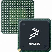
MC68EN360ZQ25VL Freescale Semiconductor, MC68EN360ZQ25VL Datasheet - Page 357

MC68EN360ZQ25VL
Manufacturer Part Number
MC68EN360ZQ25VL
Description
IC MPU QUICC 32BIT 357-PBGA
Manufacturer
Freescale Semiconductor
Datasheets
1.MC68EN302AG20BT.pdf
(8 pages)
2.MC68EN360VR25L.pdf
(14 pages)
3.MC68EN360VR25L.pdf
(2 pages)
4.MC68EN360ZQ25VL.pdf
(962 pages)
Specifications of MC68EN360ZQ25VL
Processor Type
M683xx 32-Bit
Speed
25MHz
Voltage
3.3V
Mounting Type
Surface Mount
Package / Case
357-PBGA
Family Name
M68xxx
Device Core
ColdFire
Device Core Size
32b
Frequency (max)
25MHz
Instruction Set Architecture
RISC
Supply Voltage 1 (typ)
3V
Operating Supply Voltage (max)
3.3V
Operating Supply Voltage (min)
2.7V
Operating Temp Range
0C to 70C
Operating Temperature Classification
Commercial
Mounting
Surface Mount
Pin Count
357
Package Type
BGA
Lead Free Status / RoHS Status
Contains lead / RoHS non-compliant
Features
-
Lead Free Status / Rohs Status
Not Compliant
Available stocks
Company
Part Number
Manufacturer
Quantity
Price
Company:
Part Number:
MC68EN360ZQ25VL
Manufacturer:
Freescale Semiconductor
Quantity:
10 000
- MC68EN302AG20BT PDF datasheet
- MC68EN360VR25L PDF datasheet #2
- MC68EN360VR25L PDF datasheet #3
- MC68EN360ZQ25VL PDF datasheet #4
- Current page: 357 of 962
- Download datasheet (4Mb)
7.6.2.8 CHANNEL MASK REGISTER (CMAR). The CMAR is an 8-bit, memory-mapped,
read-write register that has the same bit format as the CSR. If a bit in the CMAR is a one,
the corresponding interrupt in the CSR will be enabled. If the bit is a zero, the corresponding
interrupt in the CSR will be masked. CMAR is cleared at reset.
7.6.2.9 DATA HOLDING REGISTER (DHR). This 7-byte register serves as a buffer register
for the data being transferred during dual address IDMA cycles. No address for DHR is given
since this register cannot be addressed by the programmer. The DHR allows the data to be
packed and unpacked by the IDMA during the transfer. For example, if the source operand
size is byte and the destination operand size is word, then two-byte read cycles occur, fol-
lowed by a one-word write cycle. The two bytes of data are buffered in the DHR until the
word write cycle occurs. The DHR allows for packing and unpacking of operands for all pos-
sible combinations: bytes to words, bytes to long words, words to long words, words to
bytes, long words to bytes, and long words to words.
7.6.3 Interface Signals
The IDMA has three dedicated control signals per channel: DMA request (DREQx), DMA
acknowledge (DACKx), and end of IDMA transfer (DONEx). The peripheral used with these
signals may be either a source or a destination of the IDMA transfers.
7.6.3.1 DREQ AND DACK. These are the handshake signals between the peripheral
requiring service and the QUICC. When the peripheral requires IDMA service, it asserts
DREQx, and the QUICC begins the IDMA process. When the IDMA service is in progress,
DACKx is asserted during accesses to the device. DREQx is ignored when the IDMA is pro-
grammed to one of the internal request modes.
7.6.3.2 DONEX. This bidirectional open-drain signal is used to indicate the last IDMA trans-
fer. DONEx is always an output of the IDMA if the transfer count is exhausted.
DONEx may also operate as an input. If DONEx is externally asserted during internal
request modes, the IDMA transfer is terminated. With external request modes, DONEx may
be used as an input to the IDMA controller to indicate that the device being serviced requires
no more transfers and the transmission is to be terminated.
2. In buffer chaining or auto buffer modes, the BCR has decremented to zero, the L-bit
3. An external peripheral has asserted DONEx during an access by the IDMA to that
DONE will not be set if the channel terminates due to an error. DONE is cleared by writing
a one or by setting RST in the CMR. Writing a zero has no effect on DONE.
in the BD has been set, and no errors have occurred during any IDMA transfer bus
cycle.
peripheral and no errors have occurred during any IDMA transfer bus cycle.
DREQ must be level sensitive if IDMA uses buffer chaining
mode.
Freescale Semiconductor, Inc.
For More Information On This Product,
MC68360 USER’S MANUAL
Go to: www.freescale.com
NOTE
IDMA Channels
Related parts for MC68EN360ZQ25VL
Image
Part Number
Description
Manufacturer
Datasheet
Request
R
Part Number:
Description:
Manufacturer:
Freescale Semiconductor, Inc
Datasheet:
Part Number:
Description:
Manufacturer:
Freescale Semiconductor, Inc
Datasheet:
Part Number:
Description:
Manufacturer:
Freescale Semiconductor, Inc
Datasheet:
Part Number:
Description:
Manufacturer:
Freescale Semiconductor, Inc
Datasheet:
Part Number:
Description:
Manufacturer:
Freescale Semiconductor, Inc
Datasheet:
Part Number:
Description:
Manufacturer:
Freescale Semiconductor, Inc
Datasheet:
Part Number:
Description:
Manufacturer:
Freescale Semiconductor, Inc
Datasheet:
Part Number:
Description:
Manufacturer:
Freescale Semiconductor, Inc
Datasheet:
Part Number:
Description:
Manufacturer:
Freescale Semiconductor, Inc
Datasheet:
Part Number:
Description:
Manufacturer:
Freescale Semiconductor, Inc
Datasheet:
Part Number:
Description:
Manufacturer:
Freescale Semiconductor, Inc
Datasheet:
Part Number:
Description:
Manufacturer:
Freescale Semiconductor, Inc
Datasheet:
Part Number:
Description:
Manufacturer:
Freescale Semiconductor, Inc
Datasheet:
Part Number:
Description:
Manufacturer:
Freescale Semiconductor, Inc
Datasheet:
Part Number:
Description:
Manufacturer:
Freescale Semiconductor, Inc
Datasheet:


