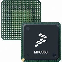
MC68EN360ZQ25VL Freescale Semiconductor, MC68EN360ZQ25VL Datasheet - Page 263

MC68EN360ZQ25VL
Manufacturer Part Number
MC68EN360ZQ25VL
Description
IC MPU QUICC 32BIT 357-PBGA
Manufacturer
Freescale Semiconductor
Datasheets
1.MC68EN302AG20BT.pdf
(8 pages)
2.MC68EN360VR25L.pdf
(14 pages)
3.MC68EN360VR25L.pdf
(2 pages)
4.MC68EN360ZQ25VL.pdf
(962 pages)
Specifications of MC68EN360ZQ25VL
Processor Type
M683xx 32-Bit
Speed
25MHz
Voltage
3.3V
Mounting Type
Surface Mount
Package / Case
357-PBGA
Family Name
M68xxx
Device Core
ColdFire
Device Core Size
32b
Frequency (max)
25MHz
Instruction Set Architecture
RISC
Supply Voltage 1 (typ)
3V
Operating Supply Voltage (max)
3.3V
Operating Supply Voltage (min)
2.7V
Operating Temp Range
0C to 70C
Operating Temperature Classification
Commercial
Mounting
Surface Mount
Pin Count
357
Package Type
BGA
Lead Free Status / RoHS Status
Contains lead / RoHS non-compliant
Features
-
Lead Free Status / Rohs Status
Not Compliant
Available stocks
Company
Part Number
Manufacturer
Quantity
Price
Company:
Part Number:
MC68EN360ZQ25VL
Manufacturer:
Freescale Semiconductor
Quantity:
10 000
- MC68EN302AG20BT PDF datasheet
- MC68EN360VR25L PDF datasheet #2
- MC68EN360VR25L PDF datasheet #3
- MC68EN360ZQ25VL PDF datasheet #4
- Current page: 263 of 962
- Download datasheet (4Mb)
Freescale Semiconductor, Inc.
System Integration Module (SIM60)
CLKO2 is always 2 CLKO1 except when the PLL is acquiring lock. When the PLL is acquir-
ing lock, the CLKO2 signal is the EXTAL or EXTAL/128 frequency, as determined by the
divide-by-128 option.
For more information see 6.9.3.9 CLKO Control Register (CLKOCR).
6.5.6 PLL Power Pins
The following pins are dedicated to the PLL operation.
6.5.6.1 VCCSYN. This pin is the V
dedicated to the analog PLL circuits. The voltage
CC
should be well regulated, and the pin should be provided with an extremely low-impedance
path to the V
power rail. VCCSYN should be bypassed to GNDSYN by a 0.1- F capacitor
CC
located as close as possible to the chip package.
6.5.6.2 GNDSYN. This pin is the GND dedicated to the analog PLL circuits. The pin should
be provided with an extremely low-impedance path to ground. GNDSYN should be
bypassed to VCCSYN by a 0.1- F capacitor located as close as possible to the chip pack-
age. The user should also bypass GNDSYN to VCCSYN with a 0.01- F capacitor as close
as possible to the chip package.
6.5.6.3 XFC. This pin connects to the off-chip capacitor for the PLL filter. One terminal of the
capacitor is connected to XFC; the other terminal is connected to VCCSYN.
6.5.7 CLKO Power Pins
The following pins are dedicated to the CLKO operation.
6.5.7.1 VCCCLK. This pin is the V
for the CLKO1 and CLKO2 output pins. The voltage
CC
should be well regulated and the pin should be provided with an extremely low-impedance
path to the V
power rail. VCCCLK should be bypassed to GNDCLK by a 0.1- F capacitor
CC
located as close as possible to the chip package.
6.5.7.2 GNDCLK. This pin is the GND for the CLKO1 and CLKO2 output pins. The pin
should be provided with an extremely low-impedance path to ground. GNDCLK should be
bypassed to VCCCLK by a 0.1- F capacitor located as close as possible to the chip pack-
age.
6.5.8 Configuration Pins (MODCK1–MODCK0)
MODCK1–MODCK0 specifies whether the PLL is enabled and what the initial VCO fre-
quency is after a hardware reset. During the assertion of RESET, the value of the MODCK1–
MODCK0 input pins causes the PLLEN bit and the MF bits of the PLLCR to be appropriately
written. MODCK1–MODCK0 also determines if the oscillator’s prescaler is used. After
RESET is negated, the MODCK1–MODCK0 pins are ignored. Table 6-1 lists the default val-
ues of the PLL. These pins have an internal pullup during a hardware reset.
MC68360 USER’S MANUAL
For More Information On This Product,
Go to: www.freescale.com
Related parts for MC68EN360ZQ25VL
Image
Part Number
Description
Manufacturer
Datasheet
Request
R
Part Number:
Description:
Manufacturer:
Freescale Semiconductor, Inc
Datasheet:
Part Number:
Description:
Manufacturer:
Freescale Semiconductor, Inc
Datasheet:
Part Number:
Description:
Manufacturer:
Freescale Semiconductor, Inc
Datasheet:
Part Number:
Description:
Manufacturer:
Freescale Semiconductor, Inc
Datasheet:
Part Number:
Description:
Manufacturer:
Freescale Semiconductor, Inc
Datasheet:
Part Number:
Description:
Manufacturer:
Freescale Semiconductor, Inc
Datasheet:
Part Number:
Description:
Manufacturer:
Freescale Semiconductor, Inc
Datasheet:
Part Number:
Description:
Manufacturer:
Freescale Semiconductor, Inc
Datasheet:
Part Number:
Description:
Manufacturer:
Freescale Semiconductor, Inc
Datasheet:
Part Number:
Description:
Manufacturer:
Freescale Semiconductor, Inc
Datasheet:
Part Number:
Description:
Manufacturer:
Freescale Semiconductor, Inc
Datasheet:
Part Number:
Description:
Manufacturer:
Freescale Semiconductor, Inc
Datasheet:
Part Number:
Description:
Manufacturer:
Freescale Semiconductor, Inc
Datasheet:
Part Number:
Description:
Manufacturer:
Freescale Semiconductor, Inc
Datasheet:
Part Number:
Description:
Manufacturer:
Freescale Semiconductor, Inc
Datasheet:


