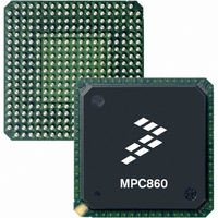
MC68EN360ZQ25VL Freescale Semiconductor, MC68EN360ZQ25VL Datasheet - Page 77

MC68EN360ZQ25VL
Manufacturer Part Number
MC68EN360ZQ25VL
Description
IC MPU QUICC 32BIT 357-PBGA
Manufacturer
Freescale Semiconductor
Datasheets
1.MC68EN302AG20BT.pdf
(8 pages)
2.MC68EN360VR25L.pdf
(14 pages)
3.MC68EN360VR25L.pdf
(2 pages)
4.MC68EN360ZQ25VL.pdf
(962 pages)
Specifications of MC68EN360ZQ25VL
Processor Type
M683xx 32-Bit
Speed
25MHz
Voltage
3.3V
Mounting Type
Surface Mount
Package / Case
357-PBGA
Family Name
M68xxx
Device Core
ColdFire
Device Core Size
32b
Frequency (max)
25MHz
Instruction Set Architecture
RISC
Supply Voltage 1 (typ)
3V
Operating Supply Voltage (max)
3.3V
Operating Supply Voltage (min)
2.7V
Operating Temp Range
0C to 70C
Operating Temperature Classification
Commercial
Mounting
Surface Mount
Pin Count
357
Package Type
BGA
Lead Free Status / RoHS Status
Contains lead / RoHS non-compliant
Features
-
Lead Free Status / Rohs Status
Not Compliant
Available stocks
Company
Part Number
Manufacturer
Quantity
Price
Company:
Part Number:
MC68EN360ZQ25VL
Manufacturer:
Freescale Semiconductor
Quantity:
10 000
- MC68EN302AG20BT PDF datasheet
- MC68EN360VR25L PDF datasheet #2
- MC68EN360VR25L PDF datasheet #3
- MC68EN360ZQ25VL PDF datasheet #4
- Current page: 77 of 962
- Download datasheet (4Mb)
SECTION 4
BUS OPERATION
This section provides a functional description of the system bus, the signals that control it,
and the bus cycles provided for data transfer operations. It also describes the error and halt
conditions, bus arbitration, and reset operation. Operation of the external bus is the same
whether the QUICC or an external device is the bus master; the names and descriptions of
bus cycles are from the viewpoint of the bus master. For exact timing specifications, refer to
Section 10 Electrical Characteristics.
The QUICC also supports the MC68EC040 (or other M68040 family members) as an exter-
nal bus master. The MC68EC040 can access QUICC registers and use QUICC peripherals.
The QUICC has a glueless MC68EC040 interface and special logic for acting as the
MC68EC040 memory controller, interrupt controller, and the provider of system protection
logic. The MC68EC040 bus operation is described in the M68040 User Manual . When the
QUICC is the bus master of an M68040 system, its bus operation remains the same when
it is the only bus master in the system. See 4.6.7 Internal Accesses for a description and
timing diagram of the MC68EC040 internal read/write cycles (i.e., MC68EC040 reading/writ-
ing the QUICC) and interrupt acknowledge cycles. See 6.11 General-Purpose Chip-Select
Overview (SRAM Banks) and 6.12 DRAM Controller Overview (DRAM Banks) for more
information on the timing diagrams of MC68EC040 DRAM and SRAM accesses.
The QUICC architecture supports byte, word, and long-word operands allowing access to
8-, 16-, and 32-bit data ports through the use of asynchronous cycles controlled by the size
outputs (SIZ1, SIZ0) and data size acknowledge inputs (DSACK1, DSACK0).
The QUICC allows byte, word, and long-word operands to be located in memory on any byte
boundary. For a misaligned transfer, more than one bus cycle may be required to complete
the transfer, regardless of port size. For a port less than 32 bits wide, multiple bus cycles
may be required for an operand transfer due to either misalignment or a port width smaller
than the operand size. Instruction words and their associated extension words must be
aligned on word boundaries. The user should be aware that misalignment of word or long-
word operands can cause the CPU32+ to perform multiple bus cycles for operand transfers;
therefore, processor performance is optimized if word and long-word memory operands are
The bus operation of the QUICC is very similar to the bus oper-
ation of the MC68030 and the MC68340. Much of the text and
figures of the bus operation of those devices is common to this
section.
Freescale Semiconductor, Inc.
Thi d
For More Information On This Product,
MC68360 USER’S MANUAL
Go to: www.freescale.com
t
NOTE
t d ith F
M k 4 0 4
Related parts for MC68EN360ZQ25VL
Image
Part Number
Description
Manufacturer
Datasheet
Request
R
Part Number:
Description:
Manufacturer:
Freescale Semiconductor, Inc
Datasheet:
Part Number:
Description:
Manufacturer:
Freescale Semiconductor, Inc
Datasheet:
Part Number:
Description:
Manufacturer:
Freescale Semiconductor, Inc
Datasheet:
Part Number:
Description:
Manufacturer:
Freescale Semiconductor, Inc
Datasheet:
Part Number:
Description:
Manufacturer:
Freescale Semiconductor, Inc
Datasheet:
Part Number:
Description:
Manufacturer:
Freescale Semiconductor, Inc
Datasheet:
Part Number:
Description:
Manufacturer:
Freescale Semiconductor, Inc
Datasheet:
Part Number:
Description:
Manufacturer:
Freescale Semiconductor, Inc
Datasheet:
Part Number:
Description:
Manufacturer:
Freescale Semiconductor, Inc
Datasheet:
Part Number:
Description:
Manufacturer:
Freescale Semiconductor, Inc
Datasheet:
Part Number:
Description:
Manufacturer:
Freescale Semiconductor, Inc
Datasheet:
Part Number:
Description:
Manufacturer:
Freescale Semiconductor, Inc
Datasheet:
Part Number:
Description:
Manufacturer:
Freescale Semiconductor, Inc
Datasheet:
Part Number:
Description:
Manufacturer:
Freescale Semiconductor, Inc
Datasheet:
Part Number:
Description:
Manufacturer:
Freescale Semiconductor, Inc
Datasheet:


