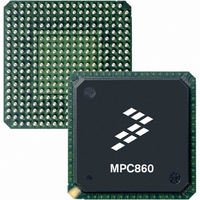
MC68EN360ZQ25VL Freescale Semiconductor, MC68EN360ZQ25VL Datasheet - Page 400

MC68EN360ZQ25VL
Manufacturer Part Number
MC68EN360ZQ25VL
Description
IC MPU QUICC 32BIT 357-PBGA
Manufacturer
Freescale Semiconductor
Datasheets
1.MC68EN302AG20BT.pdf
(8 pages)
2.MC68EN360VR25L.pdf
(14 pages)
3.MC68EN360VR25L.pdf
(2 pages)
4.MC68EN360ZQ25VL.pdf
(962 pages)
Specifications of MC68EN360ZQ25VL
Processor Type
M683xx 32-Bit
Speed
25MHz
Voltage
3.3V
Mounting Type
Surface Mount
Package / Case
357-PBGA
Family Name
M68xxx
Device Core
ColdFire
Device Core Size
32b
Frequency (max)
25MHz
Instruction Set Architecture
RISC
Supply Voltage 1 (typ)
3V
Operating Supply Voltage (max)
3.3V
Operating Supply Voltage (min)
2.7V
Operating Temp Range
0C to 70C
Operating Temperature Classification
Commercial
Mounting
Surface Mount
Pin Count
357
Package Type
BGA
Lead Free Status / RoHS Status
Contains lead / RoHS non-compliant
Features
-
Lead Free Status / Rohs Status
Not Compliant
Available stocks
Company
Part Number
Manufacturer
Quantity
Price
Company:
Part Number:
MC68EN360ZQ25VL
Manufacturer:
Freescale Semiconductor
Quantity:
10 000
- MC68EN302AG20BT PDF datasheet
- MC68EN360VR25L PDF datasheet #2
- MC68EN360VR25L PDF datasheet #3
- MC68EN360ZQ25VL PDF datasheet #4
- Current page: 400 of 962
- Download datasheet (4Mb)
Serial Interface with Time Slot Assigner
Dynamic changes mean that the routing definition of a TDM can be modified while the
SCCs/SMCs are connected to the TDM. With fixed routing, a change to the routing requires
that all SCCs/SMCs connected to the TSA be disabled, the SI routing be modified, and then
all SCCs/SMCs connected to the TSA be reenabled before the new routing takes effect.
Dynamic changes divide portions of the SI RAM into current-route RAM and shadow RAM.
Once the current-route RAM is programmed, the TSA and SI channels can be enabled, and
TSA operation can begin. When the user decides that a change in routing is required, the
user programs the shadow RAM with the new route and sets the CSRx bit in the SI CR. As
a result, the SI will exchange the shadow RAM and the current-route RAM as soon as the
corresponding sync arrives and will reset the CSRx bit to signify that the operation is com-
plete. At this time, the user may change the routing again. Note that the original current-
route RAM is now the shadow RAM and vice versa. Figure 7-28 illustrates an example of
the shadow RAM exchange process.
If one TDM with dynamic changes is programmed, the initial current-route RAM addresses
in the SI RAM are as follows:
and the shadow RAMs are at addresses:
If two TDMs with dynamic changes are programmed, the initial current-route RAM address-
es in the SI RAM are as follows:
and the shadow RAMs are at addresses:
The user can read any RAM at any time, but for proper operation of the SI, the user must
not attempt to write the current-route RAM. The user can read the SI status register (SISTR)
to find which part of the RAM is the current-route RAM.
Beyond knowing which RAM is the current-route RAM, the user may wish to know which
entry that the TSA is currently using within the current-route RAM. This information is pro-
vided in the SI RAM pointer register (SIRP). The user may also externally connect one of
the four strobes to an interrupt pin to generate an interrupt on a particular SI RAM entry start-
ing or ending execution by the TSA.
7-76
• 0–63 RXa Route
• 128–191TXa Route
• 64–127 RXa Route
• 192–255TXa Route
• 0–31 RXa Route
• 64–93 RXb Route
• 128–159TXa Route
• 192–223TXb Route
• 32–63 RXa Route
• 96–93 RXb Route
• 160–191TXa Route
• 224–255TXb Route
Freescale Semiconductor, Inc.
For More Information On This Product,
MC68360 USER’S MANUAL
Go to: www.freescale.com
Related parts for MC68EN360ZQ25VL
Image
Part Number
Description
Manufacturer
Datasheet
Request
R
Part Number:
Description:
Manufacturer:
Freescale Semiconductor, Inc
Datasheet:
Part Number:
Description:
Manufacturer:
Freescale Semiconductor, Inc
Datasheet:
Part Number:
Description:
Manufacturer:
Freescale Semiconductor, Inc
Datasheet:
Part Number:
Description:
Manufacturer:
Freescale Semiconductor, Inc
Datasheet:
Part Number:
Description:
Manufacturer:
Freescale Semiconductor, Inc
Datasheet:
Part Number:
Description:
Manufacturer:
Freescale Semiconductor, Inc
Datasheet:
Part Number:
Description:
Manufacturer:
Freescale Semiconductor, Inc
Datasheet:
Part Number:
Description:
Manufacturer:
Freescale Semiconductor, Inc
Datasheet:
Part Number:
Description:
Manufacturer:
Freescale Semiconductor, Inc
Datasheet:
Part Number:
Description:
Manufacturer:
Freescale Semiconductor, Inc
Datasheet:
Part Number:
Description:
Manufacturer:
Freescale Semiconductor, Inc
Datasheet:
Part Number:
Description:
Manufacturer:
Freescale Semiconductor, Inc
Datasheet:
Part Number:
Description:
Manufacturer:
Freescale Semiconductor, Inc
Datasheet:
Part Number:
Description:
Manufacturer:
Freescale Semiconductor, Inc
Datasheet:
Part Number:
Description:
Manufacturer:
Freescale Semiconductor, Inc
Datasheet:


