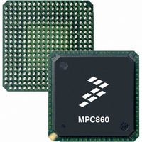
MC68EN360ZQ25VL Freescale Semiconductor, MC68EN360ZQ25VL Datasheet - Page 686

MC68EN360ZQ25VL
Manufacturer Part Number
MC68EN360ZQ25VL
Description
IC MPU QUICC 32BIT 357-PBGA
Manufacturer
Freescale Semiconductor
Datasheets
1.MC68EN302AG20BT.pdf
(8 pages)
2.MC68EN360VR25L.pdf
(14 pages)
3.MC68EN360VR25L.pdf
(2 pages)
4.MC68EN360ZQ25VL.pdf
(962 pages)
Specifications of MC68EN360ZQ25VL
Processor Type
M683xx 32-Bit
Speed
25MHz
Voltage
3.3V
Mounting Type
Surface Mount
Package / Case
357-PBGA
Family Name
M68xxx
Device Core
ColdFire
Device Core Size
32b
Frequency (max)
25MHz
Instruction Set Architecture
RISC
Supply Voltage 1 (typ)
3V
Operating Supply Voltage (max)
3.3V
Operating Supply Voltage (min)
2.7V
Operating Temp Range
0C to 70C
Operating Temperature Classification
Commercial
Mounting
Surface Mount
Pin Count
357
Package Type
BGA
Lead Free Status / RoHS Status
Contains lead / RoHS non-compliant
Features
-
Lead Free Status / Rohs Status
Not Compliant
Available stocks
Company
Part Number
Manufacturer
Quantity
Price
Company:
Part Number:
MC68EN360ZQ25VL
Manufacturer:
Freescale Semiconductor
Quantity:
10 000
- MC68EN302AG20BT PDF datasheet
- MC68EN360VR25L PDF datasheet #2
- MC68EN360VR25L PDF datasheet #3
- MC68EN360ZQ25VL PDF datasheet #4
- Current page: 686 of 962
- Download datasheet (4Mb)
Parallel I/O Ports
7.14.6 Port B Pin Functions
Refer to Table 7-20 for the description of all port B pin options. All port B pins except PB17
and PB16 may be open-drain. Port B pins are independently configured as a general-pur-
pose I/O pins if the corresponding bit in the port B pin assignment register (PBPAR) is
cleared. They are configured as dedicated on-chip peripheral pins if the corresponding
PBPAR bit is set.
When acting as a general-purpose I/O pin, the signal direction for that pin is determined by
the corresponding control bit in the port B data direction register (PBDIR). The port I/O pin
is configured as an input if the corresponding PBDIR bit is cleared; it is configured as an out-
put if the corresponding PBDIR bit is set. All PBPAR bits and PBDIR bits are cleared on total
system reset, configuring all port B pins as general-purpose input pins.
If a port B pin is selected as a general-purpose I/O pin, it may be accessed through the port
B data register (PBDAT). Data written to the PBDAT is stored in an output latch. If a port B
pin is configured as an output, the output latch data is gated onto the port pin. In this case,
when PBDAT is read, the port pin itself is read. If a port B pin is configured as an input, data
written to PBDAT is still stored in the output latch but is prevented from reaching the port
pin. In this case, when PBDAT is read, the state of the port pin is read.
All of the port B pins have more than one option. These options include on-chip peripheral
functions relating to the IDMA, Ethernet CAM interface, SPI, SMC1, SMC2, TDMa, and
TDMb.
Port B is also multiplexed with the PIP. The PIP is a CPM parallel port that can implement
fast parallel interfaces, such as Centronics. For a functional description of the dedicated pin
functions of the PIP, refer to 7.13 Parallel Interface Port (PIP).
PB3–PB5 and PB16 have an unusual property in that their on-chip peripheral functions
(BRGO4, BRGO3, BRGO2, and BRGO1) are repeated in port A. This gives an alternate way
to output the BRGO pins if other functions are used on port A. PB12–PB15 have an unusual
property in that their on-chip peripheral functions (such as RTSx or L1ST1) are repeated in
port C. This gives an alternate location to output these pins if other functions on port C are
used.
7-362
If the user does not use the PIP, the description in this section is
sufficient to describe the features of port B, and the PIP descrip-
tion does not need to be studied.
The PIP STRBI and STRBO pins are not listed in Table 7-20.
See 7.13 Parallel Interface Port (PIP) for instructions on how to
enable them.
Freescale Semiconductor, Inc.
For More Information On This Product,
MC68360 USER’S MANUAL
Go to: www.freescale.com
NOTES
Related parts for MC68EN360ZQ25VL
Image
Part Number
Description
Manufacturer
Datasheet
Request
R
Part Number:
Description:
Manufacturer:
Freescale Semiconductor, Inc
Datasheet:
Part Number:
Description:
Manufacturer:
Freescale Semiconductor, Inc
Datasheet:
Part Number:
Description:
Manufacturer:
Freescale Semiconductor, Inc
Datasheet:
Part Number:
Description:
Manufacturer:
Freescale Semiconductor, Inc
Datasheet:
Part Number:
Description:
Manufacturer:
Freescale Semiconductor, Inc
Datasheet:
Part Number:
Description:
Manufacturer:
Freescale Semiconductor, Inc
Datasheet:
Part Number:
Description:
Manufacturer:
Freescale Semiconductor, Inc
Datasheet:
Part Number:
Description:
Manufacturer:
Freescale Semiconductor, Inc
Datasheet:
Part Number:
Description:
Manufacturer:
Freescale Semiconductor, Inc
Datasheet:
Part Number:
Description:
Manufacturer:
Freescale Semiconductor, Inc
Datasheet:
Part Number:
Description:
Manufacturer:
Freescale Semiconductor, Inc
Datasheet:
Part Number:
Description:
Manufacturer:
Freescale Semiconductor, Inc
Datasheet:
Part Number:
Description:
Manufacturer:
Freescale Semiconductor, Inc
Datasheet:
Part Number:
Description:
Manufacturer:
Freescale Semiconductor, Inc
Datasheet:
Part Number:
Description:
Manufacturer:
Freescale Semiconductor, Inc
Datasheet:


