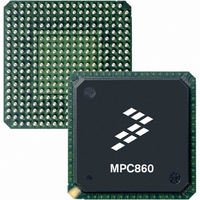
MC68EN360ZQ25VL Freescale Semiconductor, MC68EN360ZQ25VL Datasheet - Page 345

MC68EN360ZQ25VL
Manufacturer Part Number
MC68EN360ZQ25VL
Description
IC MPU QUICC 32BIT 357-PBGA
Manufacturer
Freescale Semiconductor
Datasheets
1.MC68EN302AG20BT.pdf
(8 pages)
2.MC68EN360VR25L.pdf
(14 pages)
3.MC68EN360VR25L.pdf
(2 pages)
4.MC68EN360ZQ25VL.pdf
(962 pages)
Specifications of MC68EN360ZQ25VL
Processor Type
M683xx 32-Bit
Speed
25MHz
Voltage
3.3V
Mounting Type
Surface Mount
Package / Case
357-PBGA
Family Name
M68xxx
Device Core
ColdFire
Device Core Size
32b
Frequency (max)
25MHz
Instruction Set Architecture
RISC
Supply Voltage 1 (typ)
3V
Operating Supply Voltage (max)
3.3V
Operating Supply Voltage (min)
2.7V
Operating Temp Range
0C to 70C
Operating Temperature Classification
Commercial
Mounting
Surface Mount
Pin Count
357
Package Type
BGA
Lead Free Status / RoHS Status
Contains lead / RoHS non-compliant
Features
-
Lead Free Status / Rohs Status
Not Compliant
Available stocks
Company
Part Number
Manufacturer
Quantity
Price
Company:
Part Number:
MC68EN360ZQ25VL
Manufacturer:
Freescale Semiconductor
Quantity:
10 000
- MC68EN302AG20BT PDF datasheet
- MC68EN360VR25L PDF datasheet #2
- MC68EN360VR25L PDF datasheet #3
- MC68EN360ZQ25VL PDF datasheet #4
- Current page: 345 of 962
- Download datasheet (4Mb)
GM1—Gate Mode for Pin 1
7.5.2.3 TIMER MODE REGISTER (TMR1, TMR2, TMR3, TMR4). TMR1–TMR4 are identi-
cal 16-bit, memory-mapped, read/write registers. These registers are cleared by reset.
PS—Prescaler Value
CE—Capture Edge and Enable Interrupt
OM—Output Mode
ORI—Output Reference Interrupt Enable
FRR—Free Run/Restart
This bit is only valid if the gate function is enabled in TMR1 or TMR2.
15
The prescaler is programmed to divide the clock input by values from 1 to 256. The value
00000000 divides the clock by 1; the value 11111111 divides the clock by 256.
0 = Restart gate mode. The TGATE1 pin is used to enable/disable count. A falling
1 = Normal gate mode. This mode is the same as 0, except the falling edge of TGATE1
00 = Disable interrupt on capture event; capture function is disabled.
01 = Capture on rising TINx edge only and enable interrupt on capture event.
10 = Capture on falling TINx edge only and enable interrupt on capture event.
11 = Capture on any TINx edge and enable interrupt on capture event.
0 = Active-low pulse on TOUTx for one timer input clock cycle as defined by the ICLK
1 = Toggle the TOUTx pin. TOUTx changes occur on the rising edge of the system
0 = Disable interrupt for reference reached (does not affect interrupt on capture func-
1 = Enable interrupt upon reaching the reference value.
0 = Free run. The timer count continues to increment after the reference value is
1 = Restart. The timer count is reset immediately after the reference value is reached.
14
TGATE1 pin enables and restarts the count, and a rising edge of TGATE1 disables
the count.
does not restart the count value in TCN.
bits. Thus, TOUTx may be low for one general system clock period, one general
system clock/16 period, or one TINx pin clock cycle period. TOUTx changes occur
on the rising edge of the system clock.
clock.
tion).
reached.
The TGCR should be initialized prior to the TMRs, or erratic be-
havior may occur. The only exception is the RST bit in the
TGCR, which may be modified at any time.
13
12
PS
Freescale Semiconductor, Inc.
11
For More Information On This Product,
10
MC68360 USER’S MANUAL
Go to: www.freescale.com
9
NOTE
8
7
CE
6
OM
5
ORI
4
FRR
3
2
ICLK
1
Timers
GE
0
Related parts for MC68EN360ZQ25VL
Image
Part Number
Description
Manufacturer
Datasheet
Request
R
Part Number:
Description:
Manufacturer:
Freescale Semiconductor, Inc
Datasheet:
Part Number:
Description:
Manufacturer:
Freescale Semiconductor, Inc
Datasheet:
Part Number:
Description:
Manufacturer:
Freescale Semiconductor, Inc
Datasheet:
Part Number:
Description:
Manufacturer:
Freescale Semiconductor, Inc
Datasheet:
Part Number:
Description:
Manufacturer:
Freescale Semiconductor, Inc
Datasheet:
Part Number:
Description:
Manufacturer:
Freescale Semiconductor, Inc
Datasheet:
Part Number:
Description:
Manufacturer:
Freescale Semiconductor, Inc
Datasheet:
Part Number:
Description:
Manufacturer:
Freescale Semiconductor, Inc
Datasheet:
Part Number:
Description:
Manufacturer:
Freescale Semiconductor, Inc
Datasheet:
Part Number:
Description:
Manufacturer:
Freescale Semiconductor, Inc
Datasheet:
Part Number:
Description:
Manufacturer:
Freescale Semiconductor, Inc
Datasheet:
Part Number:
Description:
Manufacturer:
Freescale Semiconductor, Inc
Datasheet:
Part Number:
Description:
Manufacturer:
Freescale Semiconductor, Inc
Datasheet:
Part Number:
Description:
Manufacturer:
Freescale Semiconductor, Inc
Datasheet:
Part Number:
Description:
Manufacturer:
Freescale Semiconductor, Inc
Datasheet:


