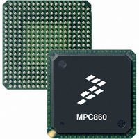
MC68EN360ZQ25VL Freescale Semiconductor, MC68EN360ZQ25VL Datasheet - Page 285

MC68EN360ZQ25VL
Manufacturer Part Number
MC68EN360ZQ25VL
Description
IC MPU QUICC 32BIT 357-PBGA
Manufacturer
Freescale Semiconductor
Datasheets
1.MC68EN302AG20BT.pdf
(8 pages)
2.MC68EN360VR25L.pdf
(14 pages)
3.MC68EN360VR25L.pdf
(2 pages)
4.MC68EN360ZQ25VL.pdf
(962 pages)
Specifications of MC68EN360ZQ25VL
Processor Type
M683xx 32-Bit
Speed
25MHz
Voltage
3.3V
Mounting Type
Surface Mount
Package / Case
357-PBGA
Family Name
M68xxx
Device Core
ColdFire
Device Core Size
32b
Frequency (max)
25MHz
Instruction Set Architecture
RISC
Supply Voltage 1 (typ)
3V
Operating Supply Voltage (max)
3.3V
Operating Supply Voltage (min)
2.7V
Operating Temp Range
0C to 70C
Operating Temperature Classification
Commercial
Mounting
Surface Mount
Pin Count
357
Package Type
BGA
Lead Free Status / RoHS Status
Contains lead / RoHS non-compliant
Features
-
Lead Free Status / Rohs Status
Not Compliant
Available stocks
Company
Part Number
Manufacturer
Quantity
Price
Company:
Part Number:
MC68EN360ZQ25VL
Manufacturer:
Freescale Semiconductor
Quantity:
10 000
- MC68EN302AG20BT PDF datasheet
- MC68EN360VR25L PDF datasheet #2
- MC68EN360VR25L PDF datasheet #3
- MC68EN360ZQ25VL PDF datasheet #4
- Current page: 285 of 962
- Download datasheet (4Mb)
PLLEN—PLL Enable Bit
The QUICC does not support disabled PLL. The bit is always set to one on reset unless the
MODCK1-MODCK0 pins are driven with 00 during reset. This mode of MODCK (00) is
reserved as indicated in 2.1.10.4 Clock Mode Select (MODCK1–MODCK0).
PLLWP—PLLCR Write Protect
PREEN—Prescaler Enable
STSIM—Stop Mode SIMCLK
MF11–MF0—Multiplication Factor
These bits define the multiplication factor that will be applied to the PLL input frequency. The
multiplication factor can be any integer from 1 to 4096. The system frequency is ((MF bits +
1)
MODCK bit configuration. The multiplication factor must be chosen to ensure that the result-
ing VCO output frequency will be in the range from 10 MHz to the maximum allowed clock
input frequency (e.g., 25 MHz for a 25-MHz device). In addition, the VCO outputs a 2 fre-
quency signal, which is 2 the multiplied value configured in the MF bits. This frequency is
not used in any of the MF calculations.
The value 000 results in a multiplier value of 1; the value $FFF results in a multiplier value
of 4096.
Anytime a new value is written into the MF11–MF0 bits, the PLL will lose the lock condition
and, after a delay, will relock. When the PLL loses its lock condition, all clocks generated by
the PLL are disabled. After a hardware reset, the MF11–MF0 bits default to either 0 or 400
($190 hex), depending on the MODCK1–MODCK0 pins (giving a multiplication factor of 1 or
401). If the multiplication factor is 401, then a standard 32.768-kHz crystal generates an ini-
This bit protects accidental writing of the PLLCR. After reset, this bit defaults to zero to
enable writing. Setting this bit prevents further writing (excluding the first write that sets
this bit).
This bit controls the divide-by-128 prescaler on the EXTAL signal. This bit is set during
hardware reset only if the MODCK1–MODCK0 pins specify that the divide-by-128 pres-
caler is used. It may be read thereafter as a status. If it is ever modified by software, it
should be changed at the same time that the corresponding change in the MF bits is per-
formed.
0 = The divide-by-128 prescaler is disabled. CLKIN = EXTAL—the PLL input clock fre-
1 = The divide-by-128 prescaler is enabled. CLKIN = EXTAL/128—the PLL input clock
0 = When the LPSTOP instruction is executed, the SIMCLK is driven from the crystal.
1 = When the LPSTOP instruction is executed, the SIM60 clock is driven from the
EXTALDIV), where EXTALDIV is either EXTAL or EXTAL/128, depending on the
quency is the EXTAL frequency.
frequency is the EXTAL frequency divided by 128.
The frequency is either EXTAL/2 or EXTAL/256, depending on the divide-by-128
option. The PLL is disabled to conserve power.
VCO.
Freescale Semiconductor, Inc.
For More Information On This Product,
MC68360 USER’S MANUAL
Go to: www.freescale.com
System Integration Module (SIM60)
Related parts for MC68EN360ZQ25VL
Image
Part Number
Description
Manufacturer
Datasheet
Request
R
Part Number:
Description:
Manufacturer:
Freescale Semiconductor, Inc
Datasheet:
Part Number:
Description:
Manufacturer:
Freescale Semiconductor, Inc
Datasheet:
Part Number:
Description:
Manufacturer:
Freescale Semiconductor, Inc
Datasheet:
Part Number:
Description:
Manufacturer:
Freescale Semiconductor, Inc
Datasheet:
Part Number:
Description:
Manufacturer:
Freescale Semiconductor, Inc
Datasheet:
Part Number:
Description:
Manufacturer:
Freescale Semiconductor, Inc
Datasheet:
Part Number:
Description:
Manufacturer:
Freescale Semiconductor, Inc
Datasheet:
Part Number:
Description:
Manufacturer:
Freescale Semiconductor, Inc
Datasheet:
Part Number:
Description:
Manufacturer:
Freescale Semiconductor, Inc
Datasheet:
Part Number:
Description:
Manufacturer:
Freescale Semiconductor, Inc
Datasheet:
Part Number:
Description:
Manufacturer:
Freescale Semiconductor, Inc
Datasheet:
Part Number:
Description:
Manufacturer:
Freescale Semiconductor, Inc
Datasheet:
Part Number:
Description:
Manufacturer:
Freescale Semiconductor, Inc
Datasheet:
Part Number:
Description:
Manufacturer:
Freescale Semiconductor, Inc
Datasheet:
Part Number:
Description:
Manufacturer:
Freescale Semiconductor, Inc
Datasheet:


